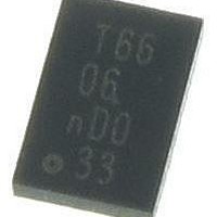
74HCT2G66GD,125 NXP Semiconductors, 74HCT2G66GD,125 Datasheet - Page 7

74HCT2G66GD,125
Manufacturer Part Number
74HCT2G66GD,125
Description
IC ANLG SWITCH SPST CMOS XSON8U
Manufacturer
NXP Semiconductors
Datasheet
1.74HC2G66DP125.pdf
(23 pages)
Specifications of 74HCT2G66GD,125
Number Of Switches
2
Switch Configuration
SPST
On Resistance (max)
142 Ohms
On Time (max)
150 ns
Off Time (max)
175 ns
Off Isolation (typ)
- 50 dB
Supply Voltage (max)
10 V
Supply Voltage (min)
2 V
Supply Current
30 mA
Maximum Power Dissipation
300 mW
Maximum Operating Temperature
+ 125 C
Mounting Style
SMD/SMT
Package / Case
XSON-8U
Minimum Operating Temperature
- 40 C
Off State Leakage Current (max)
1 uA
Operating Frequency
200 MHz
Power Dissipation
100 mW
Propagation Delay Time
80 ns
Switch Current (typ)
+/- 20 mA
Lead Free Status / RoHS Status
Lead free / RoHS Compliant
Other names
568-5446-2
Available stocks
Company
Part Number
Manufacturer
Quantity
Price
Company:
Part Number:
74HCT2G66GD,125
Manufacturer:
NXP
Quantity:
2 635
NXP Semiconductors
Table 8.
At recommended operating conditions; voltages are referenced to GND (ground 0 V); for graph see
[1]
[2]
74HC_HCT2G66
Product data sheet
Symbol
R
R
ΔR
74HCT2G66
R
R
ΔR
74HC2G66
ON(peak)
ON(rail)
ON(peak)
ON(rail)
ON
ON
At supply voltages approaching 2 V, the ON resistance becomes extremely non-linear. Therefore it is recommended that these devices
be used to transmit digital signals only, when using this supply voltage.
Typical values are measured at T
Parameter
ON resistance (peak)
ON resistance (rail)
ON resistance mismatch
between channels
ON resistance (peak)
ON resistance (rail)
ON resistance mismatch
between channels
ON resistance for 74HC2G66 and 74HCT2G66
[1]
10.2 ON resistance
amb
= 25 °C.
Conditions
V
V
V
V
V
V
V
V
I
I
I
I
I
I
I
I
All information provided in this document is subject to legal disclaimers.
I
I
I
I
I
I
I
I
I
I
I
I
V
V
V
I
I
I
V
= GND to V
= GND; see
= V
= V
= GND to V
= GND; see
= V
= V
SW
SW
SW
SW
SW
SW
SW
SW
SW
SW
SW
SW
SW
SW
SW
CC
CC
CC
CC
CC
CC
CC
CC
= 0.1 mA; V
= 1.0 mA; V
= 1.0 mA; V
= 1.0 mA; V
= 0.1 mA; V
= 1.0 mA; V
= 1.0 mA; V
= 1.0 mA; V
= 0.1 mA; V
= 1.0 mA; V
= 1.0 mA; V
= 1.0 mA; V
= 1.0 mA; V
= 1.0 mA; V
= 1.0 mA; V
= 4.5 V
= 6.0 V
= 9.0 V
= 4.5 V
Rev. 8 — 23 September 2010
; see
; see
to GND; see
to GND; see
Figure 8
Figure 8
CC
CC
Figure 8
Figure 8
; see
; see
CC
CC
CC
CC
CC
CC
CC
CC
CC
CC
CC
CC
CC
CC
CC
= 2.0 V
= 4.5 V
= 6.0 V
= 9.0 V
= 2.0 V
= 4.5 V
= 6.0 V
= 9.0 V
= 2.0 V
= 4.5 V
= 6.0 V
= 9.0 V
= 4.5 V
= 4.5 V
= 4.5 V
Figure 8
Figure 8
Figure 8
Figure 8
and
and
and
and
9
9
74HC2G66; 74HCT2G66
9
9
and
and
and
and
Dual single-pole single-throw analog switch
9
9
9
9
Min
−40 °C to +85 °C
-
-
-
-
-
-
-
-
-
-
-
-
-
-
-
-
-
-
-
Typ
250
41
30
21
65
28
22
18
65
31
23
19
41
28
31
5
4
3
5
[2]
Max
105
106
106
118
118
88
95
82
70
94
78
95
-
-
-
-
-
-
-
Figure
© NXP B.V. 2010. All rights reserved.
Min
to +125 °C
-
-
-
-
-
-
-
-
-
-
-
-
-
-
-
-
-
-
-
9.
−40 °C
Max
142
126
105
100
128
142
128
115
113
115
80
95
-
-
-
-
-
-
-
7 of 23
Unit
Ω
Ω
Ω
Ω
Ω
Ω
Ω
Ω
Ω
Ω
Ω
Ω
Ω
Ω
Ω
Ω
Ω
Ω
Ω


