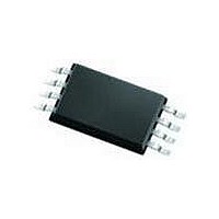
NX3L1G384GW,125 NXP Semiconductors, NX3L1G384GW,125 Datasheet - Page 3

NX3L1G384GW,125
Manufacturer Part Number
NX3L1G384GW,125
Description
IC ANALOG SWITCH SPST SOT353
Manufacturer
NXP Semiconductors
Datasheet
1.NX3L1G384GM132.pdf
(18 pages)
Specifications of NX3L1G384GW,125
Number Of Switches
1
Switch Configuration
SPST
On Resistance (max)
4.1 Ohms
On Time (max)
48 ns
Off Time (max)
21 ns
Off Isolation (typ)
- 90 dB
Supply Voltage (max)
4.3 V
Supply Voltage (min)
1.4 V
Supply Current
690 nA, 800 nA
Maximum Power Dissipation
250 mW
Maximum Operating Temperature
+ 125 C
Mounting Style
SMD/SMT
Package / Case
TSSOP-5
Minimum Operating Temperature
- 40 C
Off State Leakage Current (max)
+/- 500 nA
Operating Frequency
60 MHz
Power Dissipation
250 mW
Switch Current (typ)
+/- 350 mA
Lead Free Status / RoHS Status
Lead free / RoHS Compliant
Other names
568-5540-2
NXP Semiconductors
Table 3.
8. Functional description
Table 4.
[1]
9. Limiting values
Table 5.
In accordance with the Absolute Maximum Rating System (IEC 60134). Voltages are referenced to GND (ground = 0 V).
[1]
[2]
[3]
NX3L1G384
Product data sheet
Symbol
Y
Z
GND
E
n.c.
V
Input E
L
H
Symbol
V
V
V
I
I
I
T
P
IK
SK
SW
stg
CC
CC
I
SW
tot
H = HIGH voltage level; L = LOW voltage level.
The minimum input voltage rating may be exceeded if the input current rating is observed.
The minimum and maximum switch voltage ratings may be exceeded if the switch clamping current rating is observed but may not
exceed 4.6 V.
For TSSOP5 package: above 87.5 °C the value of P
For XSON6 package: above 118 °C the value of P
Pin description
Function table
Limiting values
Parameter
supply voltage
input voltage
switch voltage
input clamping current
switch clamping current
switch current
storage temperature
total power dissipation
7.2 Pin description
Pin
SOT353-1
1
2
3
4
-
5
[1]
Conditions
enable input E
V
V
V
source or sink current
V
pulsed at 1 ms duration, < 10 % duty cycle;
peak current
T
SOT886
1
2
3
4
5
6
amb
I
I
SW
SW
All information provided in this document is subject to legal disclaimers.
< −0.5 V
< −0.5 V or V
> −0.5 V or V
> −0.5 V or V
= −40 °C to +125 °C
tot
Rev. 4 — 7 January 2011
tot
derates linearly with 7.8 mW/K.
derates linearly with 4.0 mW/K.
I
> V
SW
SW
CC
< V
< V
Switch
ON-state
OFF-state
Description
independent input or output
independent output or input
ground (0 V)
enable input (active LOW)
not connected
supply voltage
Low-ohmic single-pole single-throw analog switch
+ 0.5 V
CC
CC
+ 0.5 V;
+ 0.5 V;
[1]
[2]
[3]
Min
−0.5
−0.5
−0.5
−50
-
-
-
−65
-
NX3L1G384
© NXP B.V. 2011. All rights reserved.
Max
+4.6
+4.6
V
-
±50
±350
±500
+150
250
CC
+ 0.5 V
3 of 18
Unit
V
V
mA
mA
mA
mA
°C
mW


