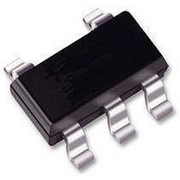
XC7SH125GW,125 NXP Semiconductors, XC7SH125GW,125 Datasheet - Page 6

XC7SH125GW,125
Manufacturer Part Number
XC7SH125GW,125
Description
IC BUS BUFFER/LINEDVR 3ST UMT5
Manufacturer
NXP Semiconductors
Datasheet
1.XC7SH125GV125.pdf
(14 pages)
Specifications of XC7SH125GW,125
Logic Type
CMOS
Number Of Channels Per Chip
1
Polarity
Non-Inverting
Supply Voltage (max)
5.5 V
Supply Voltage (min)
2 V
Maximum Operating Temperature
+ 125 C
Mounting Style
SMD/SMT
Package / Case
TSSOP-5
Lead Free Status / RoHS Status
Lead free / RoHS Compliant
NXP Semiconductors
12. Waveforms
Table 9.
XC7SH125_1
Product data sheet
Type
XC7SH125
Fig 7.
Fig 8.
Measurement points are given in
V
Input (A) to output (Y) propagation delays
Measurement points are given in
V
Enable and disable times
OL
OL
Measurement points
and V
and V
OH
OH
are typical output voltage levels that occur with the output load.
are typical output voltage levels that occur with the output load.
HIGH-to-OFF
OFF-to-HIGH
LOW-to-OFF
OFF-to-LOW
Input
V
0.5V
output
OE input
output
M
CC
Y output
A input
GND
GND
V
V
Table
V
Table
OH
CC
OL
V
I
GND
9.
9.
V
V
OH
OL
V
Rev. 01 — 4 September 2009
I
V
M
enabled
outputs
t
Output
V
0.5V
PLZ
t
PHZ
M
V
M
CC
V
M
V
X
t
PHL
V
Y
disabled
outputs
V
V
t
X
OL
PZL
t
PZH
mnb153
+ 0.3 V
t
PLH
V
M
V
M
Bus buffer/line driver; 3-state
outputs
enabled
mna644
XC7SH125
V
V
Y
OH
© NXP B.V. 2009. All rights reserved.
0.3 V
6 of 14


