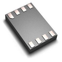
74LVC1G74GF,115 NXP Semiconductors, 74LVC1G74GF,115 Datasheet - Page 5

74LVC1G74GF,115
Manufacturer Part Number
74LVC1G74GF,115
Description
IC FLIP-FLOP SGL D S/R XSON8
Manufacturer
NXP Semiconductors
Datasheet
1.74LVC1G74DC125.pdf
(25 pages)
Specifications of 74LVC1G74GF,115
Number Of Circuits
1
Logic Family
74LVC1G74
Logic Type
Positive Edge Triggered Single D Flip Flop
Propagation Delay Time
4.1 ns, 5.9 ns, 7.1 ns, 13.4 ns
Supply Voltage (max)
5.5 V
Maximum Operating Temperature
+ 125 C
Mounting Style
SMD/SMT
Package / Case
XSON-8
Minimum Operating Temperature
- 40 C
Supply Voltage (min)
1.65 V
Lead Free Status / RoHS Status
Lead free / RoHS Compliant
Other names
568-5456-2
NXP Semiconductors
Table 3.
7. Functional description
Table 4.
[1]
Table 5.
[1]
74LVC1G74
Product data sheet
Symbol
CP
D
Q
GND
Q
RD
SD
V
Input
SD
L
H
L
Input
SD
H
H
CC
H = HIGH voltage level;
L = LOW voltage level;
X = don’t care.
H = HIGH voltage level;
L = LOW voltage level;
↑ = LOW-to-HIGH CP transition;
Q
n+1
= state after the next LOW-to-HIGH CP transition.
Pin description
Function table for asynchronous operation
Function table for synchronous operation
Pin
SOT505-2, SOT765-1, SOT833-1, SOT1089,
SOT996-2, SOT1116 and SOT1203
1
2
3
4
6
7
8
5
6.2 Pin description
RD
H
L
L
RD
H
H
CP
X
X
X
CP
↑
↑
All information provided in this document is subject to legal disclaimers.
Single D-type flip-flop with set and reset; positive edge trigger
Rev. 9 — 5 August 2010
[1]
[1]
SOT902-1
7
6
5
4
3
2
1
8
D
X
X
X
D
L
H
clock input (LOW-to-HIGH, edge-triggered)
data input
ground (0 V)
asynchronous reset-direct input (active LOW)
asynchronous set-direct input (active LOW)
Description
complement output
true output
supply voltage
Output
Q
H
L
H
Output
Q
L
H
n+1
74LVC1G74
© NXP B.V. 2010. All rights reserved.
Q
L
H
H
Q
H
L
n+1
5 of 25


