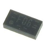
CBT3306GT,115 NXP Semiconductors, CBT3306GT,115 Datasheet - Page 4

CBT3306GT,115
Manufacturer Part Number
CBT3306GT,115
Description
IC FET BUS SWITCH DUAL XSON8
Manufacturer
NXP Semiconductors
Datasheet
1.CBT3306D118.pdf
(14 pages)
Specifications of CBT3306GT,115
Number Of Switches
Dual
Propagation Delay Time
0.25 ns
Supply Voltage (max)
5.5 V
Supply Voltage (min)
4.5 V
Maximum Operating Temperature
+ 85 C
Minimum Operating Temperature
- 40 C
Package / Case
XSON-8
Mounting Style
SMD/SMT
Off Time (max)
5 ns
On Resistance (max)
15 Ohms
On Time (max)
5 ns
Supply Current
3 uA
Lead Free Status / RoHS Status
Lead free / RoHS Compliant
Other names
568-5531-2
NXP Semiconductors
10. Static characteristics
Table 7.
Voltages are referenced to GND (ground = 0 V).
[1]
[2]
[3]
11. Dynamic characteristics
Table 8.
Voltages are referenced to GND (ground = 0 V). For test circuit see
[1]
[2]
CBT3306_5
Product data sheet
Symbol
V
I
I
V
ΔI
C
C
R
Symbol
t
t
t
I
CC
pd
en
dis
IK
pass
I
io(off)
ON
CC
All typical values are at V
This is the increase in supply current for each input that is at the specified TTL voltage level rather than V
Measured by the voltage drop between the nA and the nB terminals at the indicated current through the switch. ON resistance is
determined by the lowest voltage of the two (nA, nB) terminals.
The propagation delay is the calculated RC time constant of the typical ON resistance of the switch and the specified load capacitance,
when driven by an ideal voltage source (zero output impedance).
t
t
t
pd
en
dis
is the same as t
is the same as t
is the same as t
Parameter
input clamping voltage
input leakage current
supply current
pass voltage
additional supply current
input capacitance
off-state input/output
capacitance
ON resistance
Parameter
propagation delay
enable time
disable time
Static characteristics
Dynamic characteristics
PLH
PZL
PLZ
and t
and t
and t
CC
PZH
PHL
PHZ
= 5 V, T
.
.
.
Conditions
nA, nB to nB, nA; see
nOE to nA, nB; see
nOE to nA, nB; see
V
V
V
amb
CC
CC
CC
Conditions
V
V
V
V
output HIGH; V
I
per input pin; V
one input at 3.4 V, other inputs at
V
control pin; V
port off; V
V
V
V
O
= 25 °C.
= 5.0 V ± 0.5 V
= 5.0 V ± 0.5 V
= 5.0 V ± 0.5 V
CC
CC
CC
I
CC
CC
CC
CC
= −100 μA
= V
= 4.5 V; I
= 5.5 V; V
= 5.5 V; I
or GND
= 4.5 V; V
= 4.5 V; V
= 4.5 V; V
CC
or GND
I
= 3 V or 0 V; nOE = V
Rev. 05 — 25 March 2010
I
I
O
Figure 7
Figure 7
= 3 V or 0 V
I
I
I
I
= −18 mA
CC
I
= GND or 5.5 V
= 0 mA;
= 0 V; I
= 0 V; I
= 2.4 V; I
Figure 6
= V
= 5.5 V;
CC
I
I
= 5.0 V;
= 64 mA
= 30 mA
I
= 15 mA
Figure
CC
8.
[2]
[3]
[3]
[3]
[1][2]
[2]
[2]
Min
3.6
-
-
-
-
-
-
-
-
-
Min
1.0
1.0
−40 °C to +85 °C
-
−40 °C to +85 °C
Typ
3.15
6.45
3.9
3.4
3.4
6.8
CC
-
-
-
-
Typ
[1]
-
-
-
or GND.
CBT3306
© NXP B.V. 2010. All rights reserved.
Dual bus switch
Max
−1.2
4.2
2.5
Max
0.25
±1
15
3
5
5
5.0
5.0
-
-
Unit
V
μA
μA
V
mA
pF
pF
Ω
Ω
Ω
Unit
ns
ns
ns
4 of 14


