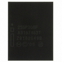
PC28F256P30BFA NUMONYX, PC28F256P30BFA Datasheet - Page 46

PC28F256P30BFA
Manufacturer Part Number
PC28F256P30BFA
Description
IC FLASH 256MBIT 100NS 64EZBGA
Manufacturer
NUMONYX
Series
Axcell™r
Datasheet
1.PF48F4000P0ZBQEF.pdf
(94 pages)
Specifications of PC28F256P30BFA
Format - Memory
FLASH
Memory Type
FLASH
Memory Size
256M (16Mx16)
Speed
100ns
Interface
Parallel
Voltage - Supply
1.7 V ~ 2 V
Operating Temperature
-40°C ~ 85°C
Package / Case
64-TBGA
Package
64EZBGA
Cell Type
NOR
Density
256 Mb
Architecture
Sectored
Block Organization
Asymmetrical
Location Of Boot Block
Bottom
Typical Operating Supply Voltage
1.8 V
Sector Size
32KByte x 4|128KByte x 255
Timing Type
Asynchronous|Synchronous
Interface Type
Parallel|Serial
Lead Free Status / RoHS Status
Lead free / RoHS Compliant
Other names
898884
898884
PC28F256P30BF 898884
898884
PC28F256P30BF 898884
Available stocks
Company
Part Number
Manufacturer
Quantity
Price
Company:
Part Number:
PC28F256P30BFA
Manufacturer:
Numonyx/Intel
Quantity:
1 871
Company:
Part Number:
PC28F256P30BFA
Manufacturer:
NUMON
Quantity:
3 161
Company:
Part Number:
PC28F256P30BFA
Manufacturer:
Micron Technology Inc
Quantity:
10 000
Part Number:
PC28F256P30BFA
Manufacturer:
INT
Quantity:
20 000
Figure 16: OTP Register Map
11.3.1
Datasheet
46
are blank. Users can program these registers as needed. Once programmed, users can
then lock the OTP Register(s) to prevent additional bit programming (see
“OTP Register Map” on page
The OTP Registers contain one-time programmable (OTP) bits; when programmed, PR
bits cannot be erased. Each OTP Register can be accessed multiple times to program
individual bits, as long as the register remains unlocked.
Each OTP Register has an associated Lock Register bit. When a Lock Register bit is
programmed, the associated OTP Register can only be read; it can no longer be
programmed. Additionally, because the Lock Register bits themselves are OTP, when
programmed, Lock Register bits cannot be erased. Therefore, when a OTP Register is
locked, it cannot be unlocked.
.
Reading the OTP Registers
The OTP Registers can be read from OTP-RA address. To read the OTP Register, first
issue the Read Device Identifier command at OTP-RA address to place the device in the
Read Device Identifier state (see
0x109
0x102
0x8A
0x91
0x89
0x88
0x85
0x84
0x81
0x80
15 14 13 12 11 10 9
15 14 13 12 11 10 9
128-bit Protection Register 16
128-bit Protection Register 1
128-Bit Protection Register 0
(Factory-Programmed)
(User-Programmable)
(User-Programmable)
(User-Programmable)
Lock Register 1
64-bit Segment
64-bit Segment
Lock Register 0
46).
8
8
Section 6.0, “Command Set” on page
7
7
6
6
5
5
4
4
3
3
2
2
1
1
0
0
Order Number: 320002-10
21). Next,
Figure 16,
P30-65nm
Mar 2010


