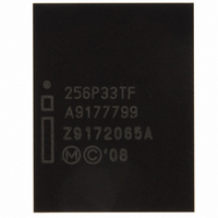
RC28F256P33TFA NUMONYX, RC28F256P33TFA Datasheet - Page 42

RC28F256P33TFA
Manufacturer Part Number
RC28F256P33TFA
Description
IC FLASH 256MBIT 95NS 64EZBGA
Manufacturer
NUMONYX
Series
Axcell™r
Specifications of RC28F256P33TFA
Format - Memory
FLASH
Memory Type
FLASH
Memory Size
256M (16Mx16)
Speed
95ns
Interface
Parallel
Voltage - Supply
2.3 V ~ 3.6 V
Operating Temperature
-40°C ~ 85°C
Package / Case
64-EZBGA
Cell Type
NOR
Density
256Mb
Interface Type
Parallel/Serial
Boot Type
Top
Address Bus
25b
Operating Supply Voltage (typ)
2.5/3/3.3V
Operating Temp Range
-40C to 85C
Package Type
EZBGA
Sync/async
Async/Sync
Operating Temperature Classification
Industrial
Operating Supply Voltage (min)
2.3V
Operating Supply Voltage (max)
3.6V
Word Size
16b
Number Of Words
32M
Supply Current
50mA
Mounting
Surface Mount
Pin Count
64
Lead Free Status / RoHS Status
Contains lead / RoHS non-compliant
Other names
902063
902063
RC28F256P33TF 902063
902063
RC28F256P33TF 902063
Available stocks
Company
Part Number
Manufacturer
Quantity
Price
Company:
Part Number:
RC28F256P33TFA
Manufacturer:
Micron Technology Inc
Quantity:
10 000
11.2.2
Note:
11.2.3
Caution:
Datasheet
42
Programming the OTP Registers
To program any of the OTP Registers, first issue the Program OTP Register command at
the parameter’s base address plus the offset to the desired OTP Register (see
6.2, “Device Command Bus Cycles” on page
data to the same OTP Register address (see
page
The device programs the 64-bit and 128-bit user-programmable OTP Register data 16
bits at a time (see
Issuing the Program OTP Register command outside of the OTP Register’s address
space causes a program error (SR.4 set). Attempting to program a locked OTP Register
causes a program error (SR.4 set) and a lock error (SR.1 set).
When programming the OTP bits in the OTP registers for a Top Parameter Device,
the following upper address bits must also be driven properly: A[Max:17] driven high
(V
Locking the OTP Registers
Each OTP Register can be locked by programming its respective lock bit in the Lock
Register. To lock a OTP Register, program the corresponding bit in the Lock Register by
issuing the Program Lock Register command, followed by the desired Lock Register
data (see
addresses of the Lock Registers are 0x80 for register 0 and 0x89 for register 1. These
addresses are used when programming the lock registers (see
Identifier Information” on page
Bit 0 of Lock Register 0 is already programmed during the manufacturing process at the
“factory”, locking the lower, pre-programmed 64-bit region of the first 128-bit OTP
Register containing the unique identification number of the device. Bit 1 of Lock
Register 0 can be programmed by the user to lock the user-programmable, 64-bit
region of the first 128-bit OTP Register. When programming Bit 1 of Lock Register 0, all
other bits need to be left as ‘1’ such that the data programmed is 0xFFFD.
Lock Register 1 controls the locking of the upper sixteen 128-bit OTP Registers. Each of
the 16 bits of Lock Register 1 correspond to each of the upper sixteen 128-bit OTP
Registers. Programming a bit in Lock Register 1 locks the corresponding 128-bit OTP
Register.
After being locked, the OTP Registers cannot be unlocked.
IH
).
41).
Section 6.2, “Device Command Bus Cycles” on page
Figure 38, “OTP Register Programming Flowchart” on page
22).
Figure 12, “OTP Register Map” on
18). Next, write the desired OTP Register
18). The physical
Table 8, “Device
Order Number: 320003-09
P33-65nm
Section
79).
Mar 2010


