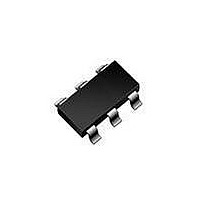
NCP1250ASN65T1G ON Semiconductor, NCP1250ASN65T1G Datasheet - Page 14

NCP1250ASN65T1G
Manufacturer Part Number
NCP1250ASN65T1G
Description
IC PWM CTLR OCP LATCH 6-TSOP
Manufacturer
ON Semiconductor
Datasheet
1.NCP1250ASN65T1G.pdf
(21 pages)
Specifications of NCP1250ASN65T1G
Output Isolation
Isolated
Frequency Range
61kHz ~ 71kHz
Voltage - Input
9.4 V ~ 28 V
Voltage - Output
12V
Operating Temperature
-40°C ~ 125°C
Package / Case
6-TSOP (0.063", 1.60mm Width)
Number Of Outputs
1
Duty Cycle (max)
84 %
Output Current
300 mA
Mounting Style
SMD/SMT
Switching Frequency
65 KHz
Operating Supply Voltage
28 V
Supply Current
2.1 mA
Maximum Operating Temperature
+ 125 C
Fall Time
30 ns
Minimum Operating Temperature
- 40 C
Rise Time
40 ns
Lead Free Status / RoHS Status
Lead free / RoHS Compliant
Available stocks
Company
Part Number
Manufacturer
Quantity
Price
Company:
Part Number:
NCP1250ASN65T1G
Manufacturer:
ON Semiconductor
Quantity:
1 250
Part Number:
NCP1250ASN65T1G
Manufacturer:
ON/安森美
Quantity:
20 000
Internal Over Power Protection
Protection (OPP), all suffering from particular problems.
These problems range from the added consumption burden
on the converter or the skip−cycle disturbance brought by
the current−sense offset. A way to reduce the power
capability at high line is to capitalize on the negative voltage
swing present on the auxiliary diode anode. During the
power switch on−time, this point dips to −NV
turns ratio between the primary winding and the auxiliary
2.5 A at low line, to 2 A at high line. This corresponds to a
20% reduction or a set point voltage of 640 mV. To reach this
Figure 41. The OPP Circuitry Affects the Maximum Peak Current Set Point by Summing a Negative Voltage to the
There are several known ways to implement Over Power
Let’s assume we need to reduce the peak current from
Figure 40. The Signal Obtained on the Auxiliary Winding Swings Negative During the On−time
Io p p
−20.0
−20.0
−40.0
−40.0
R oppL
40.0
40.0
20.0
20.0
0
0
This p oin t will
be adjusted to
reduce the ref
at hi line to the
desired level.
1 v(24)
1 v(24)
RoppU
OPP
464u
in
N
on−time
1
, N being the
(V
Internal Voltage Reference
472u
out
−N
VDD
+V
2
V
bulk
http://onsemi.com
f
)
VCC
$5%
0.8 V
aux
K2
(V O P P is negativ e)
K1
ref = 0.8 V + VOPP
14
time (s)
SUM2
480u
winding. The negative plateau observed on Figure 41 will
have an amplitude dependant on the input voltage. The idea
implemented in this chip is to sum a portion of this negative
swing with the 0.8 V internal reference level. For instance,
if the voltage swings down to −150 mV during the on time,
then the internal peak current set point will be fixed to 0.8 −
0.150 = 650 mV. The adopted principle appears in Figure 41
and shows how the final peak current set point is
constructed.
level, then the negative voltage developed on the OPP pin
must reach:
ref
off−time
from FB
488u
V
OPP
−N V in during ton
swings to:
Vout during toff
−
+
CS
+ 800m * 640m + −160 mV
reset
496u
1
1
(eq. 6)


