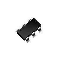
NCP1250ASN65T1G ON Semiconductor, NCP1250ASN65T1G Datasheet - Page 20

NCP1250ASN65T1G
Manufacturer Part Number
NCP1250ASN65T1G
Description
IC PWM CTLR OCP LATCH 6-TSOP
Manufacturer
ON Semiconductor
Datasheet
1.NCP1250ASN65T1G.pdf
(21 pages)
Specifications of NCP1250ASN65T1G
Output Isolation
Isolated
Frequency Range
61kHz ~ 71kHz
Voltage - Input
9.4 V ~ 28 V
Voltage - Output
12V
Operating Temperature
-40°C ~ 125°C
Package / Case
6-TSOP (0.063", 1.60mm Width)
Number Of Outputs
1
Duty Cycle (max)
84 %
Output Current
300 mA
Mounting Style
SMD/SMT
Switching Frequency
65 KHz
Operating Supply Voltage
28 V
Supply Current
2.1 mA
Maximum Operating Temperature
+ 125 C
Fall Time
30 ns
Minimum Operating Temperature
- 40 C
Rise Time
40 ns
Lead Free Status / RoHS Status
Lead free / RoHS Compliant
Available stocks
Company
Part Number
Manufacturer
Quantity
Price
Company:
Part Number:
NCP1250ASN65T1G
Manufacturer:
ON Semiconductor
Quantity:
1 250
Part Number:
NCP1250ASN65T1G
Manufacturer:
ON/安森美
Quantity:
20 000
activated, the NTC can drive the OPP pin and trigger the
adapter in case of an over temperature. During nominal
temperature if the loop is broken, the voltage runaway will
be detected and the controller will shut down the converter.
can simply be grounded.
Filtering the Spikes
to the OPP pin via the parasitic capacitances exhibited by the
In nominal V
In case the OPP pin is not used for either OPP or OVP, it
The auxiliary winding is the seat of spikes that can couple
Figure 50. A Small RC Filter Avoids the Fast Rising Spikes from Reaching the Protection Pin of the NCP1250 in
ROPPL
2.5k
ROPPL
2.5k
Figure 49. With the NTC Back in Place, the Circuit Nicely Combines OVP, OTP and OPP on the Same Pin
10
10
OPP
CC
OP P
/ output conditions, when the Zener is not
Vlatch
Vlatch
ROPPU
ROPPU
841k
NT C
841k
15V
NT C
D3
D3
15V
Presence of Energetic Perturbations Superimposed on the Input Line
11
4
5
11
4
5
1N4148
D2
1N4148
D2
1
1
OVP
OVP
http://onsemi.com
2
20
Zener diode and the series diode. To prevent an adverse
triggering of the Over Voltage Protection circuitry, it is
possible to install a small RC filter before the detection
network. Typical values are those given in Figure 50 and
must be selected to provide the adequate filtering function
without degrading the stand−by power by an excessive
current circulation.
OPP
OPP
ad d ition al fil ter
330pF
C1
VCC
VCC
9
R3
220
9
8
3
au x.
winding
aux.
winding


