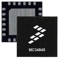
MC34845DEPR2 Freescale Semiconductor, MC34845DEPR2 Datasheet

MC34845DEPR2
Specifications of MC34845DEPR2
Related parts for MC34845DEPR2
MC34845DEPR2 Summary of contents
Page 1
... Package 12V CONTROL UNIT Figure 1. 34845 Simplified Application Diagram * This document contains certain information on a new product. Specifications and information herein are subject to change without notice. © Freescale Semiconductor, Inc., 2010. All rights reserved. 34845A/B/C/D ORDERING INFORMATION Device MC34845EP/R2 MC34845AEP/R2 MC34845BEP/R2 ...
Page 2
... V SLOPE 34845, 34845C 34845A 34845B, 34845D Min Typ Max Unit A 1.9 2.1 2.3 2.1 2.35 2.6 kHz 540 600 660 1080 1200 1320 270 300 330 V/μ 0.22 - Analog Integrated Circuit Device Data Freescale Semiconductor ...
Page 3
... VIN VDC1 VDC2 COMP VOUT EN WAKE PWM ISET Figure 2. 34845 Simplified Internal Block Diagram Analog Integrated Circuit Device Data Freescale Semiconductor INTERNAL BLOCK DIAGRAM LDO BOOST CONTROLLER V SENSE LOGIC LOW POWER MODE 6 CHANNEL CURRENT MIRROR BANDGAP CIRCUIT INTERNAL BLOCK DIAGRAM SWA ...
Page 4
... V ESD ±2000 ±200 T - 150 J T -40 to 150 S T Note 3 PPRT T 36 θ 3.1 θ 3.4 1.8 = 1500 Ω), and the = 100 pF, R ZAP ZAP Analog Integrated Circuit Device Data Freescale Semiconductor Unit °C °C °C °C °C/W °C/W W ...
Page 5
... This output is for internal use only and not to be used for other purposes 7. Minimum and maximum output voltages are dependent on Min/Max duty cycle condition. 8. Boost efficiency test is performed under the following conditions: f external components are used Analog Integrated Circuit Device Data Freescale Semiconductor STATIC AND DYNAMIC ELECTRICAL CHARACTERISTICS = mA OUT ...
Page 6
... OVP 9.0 - μS - 200 - μA - 100 - V/μ 2.88 3.0 3.12 29.4 30 30.6 V 2.011 2.043 2.074 V 0.675 0.75 0.825 % -2.0 - 2.0 -4.0 - 4.0 Analog Integrated Circuit Device Data Freescale Semiconductor ≤ A ...
Page 7
... Input High Voltage Input Current LOGIC INPUTS (EN) Input Low Voltage Input High Voltage Input Current ( LOGIC INPUTS (WAKE) Input Low Voltage Input High Voltage Input Current Analog Integrated Circuit Device Data Freescale Semiconductor STATIC AND DYNAMIC ELECTRICAL CHARACTERISTICS = mA OUT LED Symbol I CH_LEAK t /t ...
Page 8
... Boost voltage output feedback. VOUT EP EP Ground and thermal enhancement pad 34845 8 PIN CONNECTIONS VIN SWB GND SWA Figure 3. 34845 Pin Connections Definition WAKE COMP PWM ISET FAIL GND Analog Integrated Circuit Device Data Freescale Semiconductor ...
Page 9
... However for the case where the PWM and ENABLE signals are applied before VIN, the ramp up time of VIN between 0V and 5V should be no longer than 2ms. Analog Integrated Circuit Device Data Freescale Semiconductor FUNCTIONAL DESCRIPTION INTRODUCTION portable equipment compared to CCFL. In large size panels, ...
Page 10
... Once a failure is detected, the FAIL pin can be cleared by recycling the EN pin or applying a complete power-on-reset (POR). If the detected failure is an Over- current time-out, the EN pin or a POR must be cycled/ executed to restart the part. , then the device shuts down all functions. Analog Integrated Circuit Device Data Freescale Semiconductor ...
Page 11
... Figure 7. Typical ILED Dimming Linearity (FPWM=25kHz) Analog Integrated Circuit Device Data Freescale Semiconductor Vin= 600kHz L=10uH, 68mOhm (IHLP2525CZER100M01) Schottky 5A, 100V (PDS5100HDICT-ND) COUT = 2x2.2µF FPWM=25kHz Load = 9 LEDs, 20mA/channel VLED = 27.8V, ±0.5V /channel ...
Page 12
... VOUT (ac coupled) VOUT (ac coupled) VCH1 VCH1 ILED1 ILED1 Figure 8. Typical Operating Waveforms (FPWM=25kHz, 50% duty) PWM PWM VOUT (ac coupled) VOUT (ac coupled) VCH1 VCH1 ILED1 ILED1 Figure 9. Low Duty Dimming Operation Waveforms (FPWM=25 kHz, 1% duty) 34845 12 Analog Integrated Circuit Device Data Freescale Semiconductor ...
Page 13
... EP 21 7.65kΩ 765KΩ GND GND 0.1 % Figure 10. Typical Application Circuit for Single Wire Control 9.0V, I /channel = 20 mA/channel, 10 LEDs/channel, OVP = 35V LED Analog Integrated Circuit Device Data Freescale Semiconductor TYPICAL APPLICATIONS 4.7 uF 4.7 uF 10uf 25V 100 pF 100pF SWA 4 SWB 3 VOU T ...
Page 14
... LED LED LEG 1 LEG 2 LEG 3 LEG 4 LEG 5 LEG 6 100 pF 100 pF 100p F = 1.2 MHz S = 3.3V) PWM LED LED LED LED LED LED LEG 1 LEG 2 LEG 3 LEG 4 LEG 5 LEG 6 100 pF 100pF 100 pF = 300 kHz S = 3.3V) PWM Analog Integrated Circuit Device Data Freescale Semiconductor ...
Page 15
... Network Compensation Since this Boost converter is current controlled, a Type II compensation is needed. Analog Integrated Circuit Device Data Freescale Semiconductor COMPONENTS CALCULATION Note that before calculating the network compensation, all boost converter components need to be known. For this type of compensation it is recommended to push out the Right Half Plane Zero to higher frequencies where it will not significantly affect the overall loop ...
Page 16
... Isat min = 2.6A Cin(min) Cout(min) Rcomp at Rshunt at Ccomp1 Ccomp2 V V PWM=3.3V PWM=3.3V 1x10uF 4.7uF; 3.3kOhm 10kOhm 33nF 220pF X7R; 25V X7R; 50V 1x10uF 2.2uF; 2kOhm 16kOhm 56nF 220pF X7R; 25V X7R; 100V Analog Integrated Circuit Device Data Freescale Semiconductor ...
Page 17
... For the most current package revision, visit www.freescale.com and perform a keyword search using the “98A” listed below. Analog Integrated Circuit Device Data Freescale Semiconductor PACKAGING PACKAGE DIMENSIONS EP SUFFIX 24-PIN 98ASA00087D REVISION A PACKAGING PACKAGE DIMENSIONS 34845 17 ...
Page 18
... PACKAGING PACKAGE DIMENSIONS 34845 18 EP SUFFIX 24-PIN 98ASA00087D REVISION A Analog Integrated Circuit Device Data Freescale Semiconductor ...
Page 19
... Analog Integrated Circuit Device Data Freescale Semiconductor EP SUFFIX 24-PIN 98ASA00087D REVISION A PACKAGING 34845 19 ...
Page 20
... Freescale Semiconductor was negligent regarding the design or manufacture of the part. Freescale™ and the Freescale logo are trademarks of Freescale Semiconductor, Inc ...


