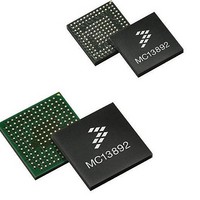
MC13892BJVL Freescale Semiconductor, MC13892BJVL Datasheet - Page 7

MC13892BJVL
Manufacturer Part Number
MC13892BJVL
Description
IC PMU I.MX51/37/35/27 186MAPBGA
Manufacturer
Freescale Semiconductor
Datasheets
1.MC13892AJVLR2.pdf
(156 pages)
2.MC13892AJVLR2.pdf
(2 pages)
3.MC13892AJVLR2.pdf
(16 pages)
4.MC13892AJVLR2.pdf
(5 pages)
Specifications of MC13892BJVL
Applications
Battery Management, Display (LED Drivers), Handheld/Mobile Devices, Power Supply
Operating Temperature
-40°C ~ 85°C
Mounting Type
Surface Mount
Package / Case
186-LFBGA
Mounting Style
SMD/SMT
Duty Cycle (max)
55 %
Input Voltage
- 0.3 V to + 20 V
Maximum Operating Temperature
+ 85 C
Minimum Operating Temperature
- 30 C
Output Current
30 mA
Output Voltage
3.3 V
Topology
Boost
Lead Free Status / RoHS Status
Lead free / RoHS Compliant
Current - Supply
-
Voltage - Supply
-
Lead Free Status / Rohs Status
Lead free / RoHS Compliant
Available stocks
Company
Part Number
Manufacturer
Quantity
Price
Company:
Part Number:
MC13892BJVL
Manufacturer:
Freescale Semiconductor
Quantity:
10 000
Company:
Part Number:
MC13892BJVLR2
Manufacturer:
Freescale Semiconductor
Quantity:
10 000
Table 2. 13892 Pin Definitions (continued)
Analog Integrated Circuit Device Data
Freescale Semiconductor
Pin Number
13982VK
7x7 mm
A functional description of each pin can be found in the Functional Pin Description section beginning on
on the
D10
D12
D13
E10
E11
E12
E13
D1
D2
D4
D5
D6
D7
D8
D9
E1
E2
E4
E5
E6
E7
E8
E9
F1
F2
F4
F5
F6
Pin Number on
A6, B3, B4, D3,
D4, E4, E5, E6
the 13982VL
12x12 mm
G13, G14
G1, G2
B10
C10
C11
C12
D11
B12
D10
E11
D13
E13
G3
D1
C1
C3
D7
B7
B8
E1
D2
C5
D6
B6
C8
F2
C7
CHRGSE1B
GNDCHRG
REFCORE
CHRGLED
SWBSTFB
GNDSUB1
Pin Name
BATTFET
PWRON1
PWRON2
GNDSW1
GNDSW3
GNDLED
VBUSEN
ADTRIG
LEDMD
LICELL
BPSNS
UVBUS
PUMS2
SW3FB
LEDAD
VUSB
LEDG
DVS1
VPLL
VSD
UID
INT
Rating
3.6
3.6
3.6
3.6
3.6
3.6
3.6
4.8
4.8
3.6
3.6
7.5
5.5
3.6
3.6
3.6
3.6
3.6
3.6
(V)
28
20
20
28
-
-
-
-
-
Pin Function
Ground
Ground
Ground
Ground
Ground
Output
Output
Output
Output
Output
Output
Output
Input
Input
Input
Input
Input
Input
Input
Input
Input
Input
Input
Input
Input
Input
I/O
I/O
Voltage Supply for PLL Output regulator processor PLL
Power Up Mode Select
PWM Driver for Green
Auxiliary Display LED Auxiliary display backlight LED sinking
Coin Cell Connection
Switcher 3 Feedback
Battery Plus Sense
Switcher 1 Ground
Switcher 3 Ground
Dynamic Voltage
Scaling Control 1
SD Card Supply
Charger Ground
Core Reference
Interrupt Signal
Switcher Boost
Charger Select
Formal Name
VBUS Enable
Charger LED
LED Ground
ADC Trigger
USB Supply
Battery FET
Power On 1
Power On 2
Connection
LED Driver
Feedback
Ground 1
USB Bus
USB ID
LED
2
USB transceiver regulator output
Output regulator SD card
Switcher BST feedback
Main display backlight LED current sink
driver
Switcher 1DVS input pin
Main bandgap reference
Charger forced SE1 detection input
1. Coin cell supply input
2. Coin cell charger output
Driver output for battery path FET M3
1. BP sense point
2. Charge current sensing point 2
Power on/off button connection 1
1. USB transceiver cable interface
2. VBUS & OTG supply output
General purpose LED current sink driver
Green
Ground for LED drivers
USB OTG transceiver cable ID
Power up mode supply setting 2
Ground for charger interface
Trickle LED driver output 1
Power on/off button connection 2
ADC trigger input
Interrupt to processor
Ground for switcher 1
Ground for switcher 3
External VBUS enable pin for OTG supply
Switcher 3 feedback
current driver
Non critical signal ground and thermal heat
sink
Definition
page
PIN CONNECTIONS
32.
13892
7


