NCP5393MNR2G ON Semiconductor, NCP5393MNR2G Datasheet - Page 8
NCP5393MNR2G
Manufacturer Part Number
NCP5393MNR2G
Description
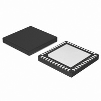
IC CTLR 2/3/4PHASE CPU 48-QFN
Manufacturer
ON Semiconductor
Datasheet
1.NCP5393MNR2G.pdf
(23 pages)
Specifications of NCP5393MNR2G
Applications
Multiphase Controller
Current - Supply
25mA
Voltage - Supply
4.75 V ~ 5.25 V
Operating Temperature
0°C ~ 70°C
Mounting Type
Surface Mount
Package / Case
48-TQFN Exposed Pad
Mounting Style
SMD/SMT
Lead Free Status / RoHS Status
Lead free / RoHS Compliant
Available stocks
Company
Part Number
Manufacturer
Quantity
Price
Company:

Part Number:
NCP5393MNR2G
Manufacturer:
RFMD
Quantity:
10 000
Part Number:
NCP5393MNR2G
Manufacturer:
ON
Quantity:
20 000


ELECTRICAL CHARACTERISTICS
ERROR AMPLIFIERS (V
DIFFERENTIAL SUMMING AMPLIFIERS (V
DROOP AMPLIFIERS (V
3. Guaranteed by design. Not production tested.
Input Bias Current
Input Offset Voltage (Note 3)
Open Loop DC Gain
Open Loop Unity Gain Bandwidth
Open Loop Phase Margin
Slew Rate
Maximum Output Voltage
Minimum Output Voltage
Output Source Current (Note 3)
Output Sink Current (Note 3)
VS- Input Bias Current
VS+ Input Resistance
VS+ Input Bias Voltage
VS+ Input Voltage Range (Note 3)
VS- Input Voltage Range (Note 3)
-3dB Bandwidth (Note 3)
DC gain, VS+ to DIFFOUT
DAC Accuracy (Measured at VS+)
Slew Rate
Maximum Output Voltage
Minimum Output Voltage
Output source current (Note 3)
Output sink current (Note 3)
Gain from Current Sense Input to
Droop Amplifier Output
Droop Amplifier DC Output Voltage
Slew Rate
Maximum Output Voltage
Minimum Output Voltage
Output Source Current (Note 3)
Output Sink Current (Note 3)
Parameter
DD
DD
& V
& V
DDNB
DDNB
)
)
V+ = V- = 1.3V
C
C
C
DV
1.5 V < V
C
10 mV of Overdrive, I
10 mV of Overdrive, I
10 mV of Overdrive, V
10 mV of Overdrive, V
VS- Voltage at 0 V
DRVON = Low
DRVON = High
DRVON = Low
DRVON = High
C
VS+ to VS- = 0.5 V to 2.35 V
Closed Loop Measurement, Error Amplifier Inside the
Loop.
1.0125 V v VDAC v 1.5500 V
0.8000 V v VDAC v 1.0000 V
12.5 mV v VDAC v 0.8000 V
DV
I
I
V
V
0 mV < (CSx - CSxN) < 60 mV
CSx = CSxN = 1.3 V
C
I
I
V
V
SOURCE
SINK
SOURCE
SINK
(Unless otherwise stated: 0°CvT
OUT
OUT
OUT
OUT
L
L
L
L
L
L
IN
IN
= 60 pF to GND, R
= 60 pF to GND, R
= 60 pF to GND, R
= 60 pF, DC Loading = $125 mA
= 80 pF to GND, R
= 20 pF to GND, R
DD
= 100 mV, AV = -10 V/V,
= 100 mV, DV
= 2 mA
= 1.0 mA
= 3 V
= 0.5 V
= 3.0 V
= 1.0 V
& V
= 2 mA
= 4.0 mA
COMP
DDNB
< 2.5 V,
http://onsemi.com
)
Test Conditions
OUT
NCP5393
SOURCE
SINK
L
L
L
L
L
OUT
OUT
= 10 kW to GND
= 10 kW to GND
= 10 kW to GND
= 10 kW to GND
= 1 kW to GND
= 1.3 V-1.2 V
8
= 2.0 mA
= 3.5 V
= 1.0 V
= 2.0 mA
A
v70°C; 4.75 VvV
CC
v5.25 V; All DAC Codes; C
0.982
-200
-1.0
-0.3
-0.3
-0.5
Min
3.5
2.0
5.7
3.0
-5
-8
-
-
-
-
-
-
-
-
-
-
0.37
0.05
Typ
1.0
1.0
2.0
2.0
6.0
1.3
5.0
4.0
1.0
80
15
70
33
15
10
-
-
5
-
-
2
2
7
-
-
-
-
-
-
-
1.022
Max
VCC
200
1.0
1.0
3.0
0.3
0.5
0.5
6.3
1.0
-
-
-
-
-
-
-
5
8
-
-
-
-
= 0.1 mF)
MHz
V/ms
MHz
V/ms
V/ms
Unit
deg
V/V
V/V
mV
mA
mA
mV
mV
mA
mA
mA
mA
nA
dB
kW
mA
%
V
V
V
V
V
V
V
V
V
V
Related parts for NCP5393MNR2G
Image
Part Number
Description
Manufacturer
Datasheet
Request
R

Part Number:
Description:
2/3/4-Phase Controller
Manufacturer:
ON Semiconductor
Datasheet:
Part Number:
Description:
ON Semiconductor [VOLTAGE REGULATOR]
Manufacturer:
ON Semiconductor
Datasheet:
Part Number:
Description:
357-036-542-201 CARDEDGE 36POS DL .156 BLK LOPRO
Manufacturer:
ON Semiconductor
Datasheet:
Part Number:
Description:
357-036-542-201 CARDEDGE 36POS DL .156 BLK LOPRO
Manufacturer:
ON Semiconductor
Datasheet:
Part Number:
Description:
357-036-542-201 CARDEDGE 36POS DL .156 BLK LOPRO
Manufacturer:
ON Semiconductor
Datasheet:
Part Number:
Description:
357-036-542-201 CARDEDGE 36POS DL .156 BLK LOPRO
Manufacturer:
ON Semiconductor
Datasheet:
Part Number:
Description:
357-036-542-201 CARDEDGE 36POS DL .156 BLK LOPRO
Manufacturer:
ON Semiconductor
Datasheet:
Part Number:
Description:
357-036-542-201 CARDEDGE 36POS DL .156 BLK LOPRO
Manufacturer:
ON Semiconductor
Datasheet:
Part Number:
Description:
357-036-542-201 CARDEDGE 36POS DL .156 BLK LOPRO
Manufacturer:
ON Semiconductor
Datasheet:
Part Number:
Description:
357-036-542-201 CARDEDGE 36POS DL .156 BLK LOPRO
Manufacturer:
ON Semiconductor
Datasheet:
Part Number:
Description:
357-036-542-201 CARDEDGE 36POS DL .156 BLK LOPRO
Manufacturer:
ON Semiconductor
Datasheet:
Part Number:
Description:
357-036-542-201 CARDEDGE 36POS DL .156 BLK LOPRO
Manufacturer:
ON Semiconductor
Datasheet:
Part Number:
Description:
Manufacturer:
ON Semiconductor
Datasheet:
Part Number:
Description:
Manufacturer:
ON Semiconductor
Datasheet: