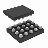
LP8720TLX-B/NOPB National Semiconductor, LP8720TLX-B/NOPB Datasheet - Page 18

LP8720TLX-B/NOPB
Manufacturer Part Number
LP8720TLX-B/NOPB
Description
IC REG BUCK 5-LDO I2C 20USMD
Manufacturer
National Semiconductor
Datasheet
1.LP8720TLENOPB.pdf
(24 pages)
Specifications of LP8720TLX-B/NOPB
Topology
Step-Down (Buck) Synchronous (1), Linear (LDO) (5)
Function
Any Function
Number Of Outputs
6
Frequency - Switching
2MHz
Voltage/current - Output 1
0.8 V ~ 2.3 V, 400mA
Voltage/current - Output 2
1.2 V ~ 3.3 V, 300mA
Voltage/current - Output 3
1.2 V ~ 3.3 V, 300mA
W/led Driver
No
W/supervisor
No
W/sequencer
Yes
Voltage - Supply
2.7 V ~ 4.5 V
Operating Temperature
-40°C ~ 85°C
Mounting Type
Surface Mount
Package / Case
20-UFBGA
Lead Free Status / RoHS Status
Lead free / RoHS Compliant
Available stocks
Company
Part Number
Manufacturer
Quantity
Price
Part Number:
LP8720TLX-B/NOPB
Manufacturer:
TI/德州仪器
Quantity:
20 000
www.national.com
f
t
t
t
t
t
t
t
t
t
CLK
BF
HOLD
CLK-LP
CLK-HP
SU
DATA-HOLD
DATA-SU
SU
TRANS
Serial Interface
Unless otherwise noted, V
values and limits appearing in normal type apply for T
temperature range for operation, T
Symbol
Notes to Electrical Characteristics Tables
Note 1: Absolute Maximum Ratings are limits beyond which damage to the device may occur. Operating Ratings are conditions under which operation of the
device is guaranteed. Operating Ratings do not imply guaranteed performance limits. For guaranteed performance limits and associated test conditions, see the
Electrical Characteristics tables.
Note 2: All voltages are with respect to the potential at the GND pin.
Note 3: The Absolute Maximum power dissipation depends on the ambient temperature and can be calculated using the formula
P = (T
where T
Absolute Maximum Ratings results from substituting the Absolute Maximum junction temperature, 150ºC for T
can be dissipated safely at ambient temperatures below 70°C. Less power can be dissipated safely at ambient temperatures above 70°C. The Absolute Maximum
power dissipation can be increased by 22mW for each degree below 70°C, and it must be de-rated by 22 mW for each degree above 70ºC.
Note 4: The human-body model is 100 pF discharged through 1.5 kΩ. The machine model is a 200 pF capacitor discharged directly into each pin, MIL-STD-883
3015.7.
Note 5: Like the Absolute Maximum power dissipation, the maximum power dissipation for operation depends on the ambient temperature. The 1.2W rating for
Micro SMD 20 appearing under Operating Ratings results from substituting the maximum junction temperature for operation, 125°C, for T
C/W for θ
70°C. The maximum power dissipation for operation can be increased by 22mW for each degree below 70°C, and it must be de-rated by 22 mW for each degree
above 70°C.
Note 6: All limits are guaranteed. All electrical characteristics having room-temperature limits are tested during production with T
are guaranteed by correlating the electrical characteristics to process and temperature variations and applying statistical process control.
Note 7: Guaranteed by design.
Note 8: Dropout voltage is the input-to-output voltage difference at which the output voltage is 100mV below its nominal value. This specification does not apply
in cases it implies operation with an input voltage below the 2.5V minimum appearing under Operating Ratings. For example, this specification does not apply
for devices having 1.5V outputs because the specification would imply operation with an input voltage at or about 1.5V.
Note 9: Junction-to-ambient thermal resistance is highly application and board-layout dependent. In applications where high maximum power dissipation exists,
special care must be paid to thermal dissipation issues in board design.
Note 10: Guaranteed for output voltages no less than 1.0V
J
– T
J
JA
is the junction temperature, T
A
into (eg. 1) above. More power can be dissipated at ambient temperatures below 70°C. Less power can be dissipated at ambient temperatures above
)/θ
Clock Frequency
Bus-Free Time between START
and STOP
Hold Time Repeated START
Condition
CLK Low Period
CLK High Period
Set-Up Time Repeated START
Condition
Data Hold Time
Data Set-Up Time
Set-Up Time for STOP Condition
Maximum Pulse Width of Spikes
that Must Be Suppressed by the
Input Filter of Both DATA & CLK
Signals
JA
, (eq. 1)
Parameter
VBATT
=V
A
is the ambient temperature, and θ
VINB
J
= -40 to +125°C.
=V
VIN1
=V
VIN2
=3.6V, GND=GNDB=0V, C
(Note
J
=25°C. Limits appearing in boldface type apply over the entire junction
6,
Conditions
JA
Note
is the junction-to-ambient thermal resistance. The 1.75W rating appearing under
18
7)
VBATT
=C
VIN1
Typ
50
J
, 70ºC for T
=C
VIN2
=2.2 µF, C
A
Min
100
1.3
0.6
1.3
0.6
0.6
0.6
50
, and 45°C/W for θ
J
= 25°C. All hot and cold limits
Limit
VINB
J
, 70°C for T
Max
=10 µF. Typical
400
JA
. More power
A
, and 45°
Units
kHz
µs
µs
µs
µs
µs
ns
ns
µs
ns


