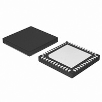
ADP3212MNR2G ON Semiconductor, ADP3212MNR2G Datasheet - Page 20

ADP3212MNR2G
Manufacturer Part Number
ADP3212MNR2G
Description
IC CTLR BUCK 7BIT 2PHASE 48QFN
Manufacturer
ON Semiconductor
Datasheet
1.NCP3218MNR2G.pdf
(35 pages)
Specifications of ADP3212MNR2G
Applications
Controller, Intel IMVP-6.5™
Voltage - Input
3.3 V ~ 22 V
Number Of Outputs
1
Voltage - Output
0.3 V ~ 1.5V
Operating Temperature
-40°C ~ 100°C
Mounting Type
Surface Mount
Package / Case
48-TFQFN Exposed Pad
Output Voltage
0.9512 V
Output Current
52 A
Input Voltage
8 V to 19 V
Supply Current
7 mA
Switching Frequency
300 KHz
Mounting Style
SMD/SMT
Maximum Operating Temperature
+ 100 C
Minimum Operating Temperature
- 40 C
Lead Free Status / RoHS Status
Lead free / RoHS Compliant
Available stocks
Company
Part Number
Manufacturer
Quantity
Price
Company:
Part Number:
ADP3212MNR2G
Manufacturer:
ON Semiconductor
Quantity:
950
Part Number:
ADP3212MNR2G
Manufacturer:
ON/安森美
Quantity:
20 000
APD3212/NCP3218/NCP3218G shuts off. In shutdown
mode, the controller holds the PWM outputs low, shorts the
capacitors of the SS and PGDELAY pins to ground, and
drives the DRVH and DRVL outputs low.
during startup and shutdown of the APD3212/NCP3218/
NCP3218G. All input pins must be at ground prior to
removing or applying VCC, and all output pins should be
left in high impedance state while VCC is off.
Thermal Throttling Control
monitoring circuit to detect whether the temperature of the
VR has exceeded a user−defined thermal throttling
threshold. The thermal monitoring circuit requires an
external resistor divider connected between the VCC pin
and GND. The divider consists of an NTC thermistor and a
resistor. To generate a voltage that is proportional to
temperature, the midpoint of the divider is connected to the
Table 3. VID CODE TABLE
The user must adhere to proper power−supply sequencing
The APD3212/NCP3218/NCP3218G includes a thermal
VID6
0
0
0
0
0
0
0
0
0
0
0
0
0
0
0
0
0
0
0
0
0
0
0
0
0
0
0
0
0
0
0
VID5
0
0
0
0
0
0
0
0
0
0
0
0
0
0
0
0
0
0
0
0
0
0
0
0
0
0
0
0
0
0
0
VID4
0
0
0
0
0
0
0
0
0
0
0
0
0
0
0
0
0
1
1
1
1
1
1
1
1
1
1
1
1
1
1
VID3
0
0
0
0
0
0
0
0
0
1
1
1
1
1
1
1
1
0
0
0
0
0
0
0
0
1
1
1
1
1
1
http://onsemi.com
VID2
0
0
0
0
0
1
1
1
1
0
0
0
0
1
1
1
1
0
0
0
0
1
1
1
1
0
0
0
0
1
1
20
TTSNS pin. An internal comparator circuit compares the
TTSNS voltage to half the VCC threshold and outputs a
logic level signal at the VRTT output when the temperature
trips the user−set alarm threshold. The VRTT output is
designed to drive an external transistor that in turn provides
the high current, open−drain VRTT signal required by the
IMVP−6.5 specification. The internal VRTT comparator
has a hysteresis of approximately 100 mV to prevent high
frequency oscillation of VRTT when the temperature
approaches the set alarm point.
Output Current Monitor
current monitor. The IMON pin sources a current
proportional to the inductor current. A resistor from IMON
pin to FBRTN sets the gain. A 0.1 mF is added in parallel with
R
to prevent it from going above 1.15 V.
VID1
MON
The APD3212/NCP3218/NCP3218G has an output
0
0
0
1
1
0
0
1
1
0
0
1
1
0
0
1
1
0
0
1
1
0
0
1
1
0
0
1
1
0
0
to filter the inductor ripple. The IMON pin is clamped
VID0
0
0
1
0
1
0
1
0
1
0
1
0
1
0
1
0
1
0
1
0
1
0
1
0
1
0
1
0
1
0
1
Output (V)
1.5000 V
1.5000 V
1.4875 V
1.4750 V
1.4625 V
1.4500 V
1.4375 V
1.4250 V
1.4125 V
1.4000 V
1.3875 V
1.3750 V
1.3625 V
1.3500 V
1.3375 V
1.3250 V
1.3125 V
1.3000 V
1.2875 V
1.2750 V
1.2625 V
1.2500 V
1.2375 V
1.2250 V
1.2125 V
1.2000 V
1.1875 V
1.1750 V
1.1625 V
1.1500 V
1.1375 V


