LMP90100EB/NOPB National Semiconductor, LMP90100EB/NOPB Datasheet - Page 9
LMP90100EB/NOPB
Manufacturer Part Number
LMP90100EB/NOPB
Description
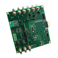
EVAL BOARD FOR LMP90100
Manufacturer
National Semiconductor
Datasheet
1.LMP90100EBNOPB.pdf
(30 pages)
Specifications of LMP90100EB/NOPB
Main Purpose
Interface, Analog Front End (AFE)
Embedded
No
Utilized Ic / Part
LMP90100
Primary Attributes
8 Programmable Output Data Rates Per Channel
Secondary Attributes
SPI Interface
Silicon Manufacturer
National
Silicon Core Number
LMP90100
Kit Application Type
Data Converter
Application Sub Type
ADC
Kit Contents
LMP90100 Evaluation Board
Lead Free Status / RoHS Status
Lead free / RoHS Compliant


© 2009 National Semiconductor Corporation
H. Connecting and Powering the Boards
I.
1.
2.
3.
Configuring the Device Using the Sensor AFE Software
1.
Connect the LMP90100EB’s JP12 to SPIO-4 Board’s J6 (pins 1-16) as seen in Figure 3.
Connect SPIO-4 Board to a PC via USB.
Use a multimeter to measure LMP90100EB’s JP6, JP7, and JP14.P2; they should all be approximately
5V. If they are not, check your power supplies and jumpers.
Follow the step-by-step instructions under the “HelpBar” mini-tab to configure the device. The
recommended configuration can be seen in Figure 7.
a.
b.
c.
d.
e.
f.
g.
h.
i.
Step 1: Select a Sensor - select “DC” “DC” since the input source is a DC voltage
Step 2: Configure Inputs – click on the “INPUT MUX” block to set “VINP = 000: VIN0” and
“VINN = 000: VIN0”. Since VINP = VINN, a reading of approximately 0V should be read.
Step 3: Select Reference – click on the “VREF MUX” block to choose “VREF_SEL = 0: VREF1”.
On the left hand side of the GUI, change the VREF1 value to 5.0V as seen below.
Step 4: Source IB1/IB2? – this step can be ignored because neither IB1 nor IB2 is connected to the
inputs.
Step 5: Set Gain – since VIN = 0V, the maximum gain that can be set is 128x. Click on the “FGA”
block, “PGA” block, or the “Gain” slider to select the gain.
Step 6: Set Buffer – click on the “BUFF” block to include or exclude the buffer from the signal path.
Step 7: Set Calibration - the purpose of this example is to show how the LMP90100 removes the
offset error using background calibration. Initially, disable the calibration by selecting “000: No
Calibration” under the “No Calibration” block.
Refer to the LMP90100 datasheet to more information on the LMP90100’s background calibration
types and modes.
Step 8: Int/Ext CLK? – click on the “CLK MUX” block and make sure the internal clock is selected.
Step 9: Performance - click on the “Performance” mini-tab. This tab displays the Estimated
Device Performance base on the block diagram that you’ve configured, as well as the Measured
System Performance if you’ve connected a board and ran the LMP90100.
Page 9 of 30
with Sensor AFE Software User’s Guide
lmp90100eb_usersguide_20101227_v23.doc
LMP90100 Evaluation Board
Related parts for LMP90100EB/NOPB
Image
Part Number
Description
Manufacturer
Datasheet
Request
R

Part Number:
Description:
National Semiconductor [8-Bit D/A Converter]
Manufacturer:
National Semiconductor
Datasheet:
Part Number:
Description:
National Semiconductor [Media Coprocessor]
Manufacturer:
National Semiconductor
Datasheet:
Part Number:
Description:
Digitally Controlled Tone and Volume Circuit with Stereo Audio Power Amplifier, Microphone Preamp Stage and National 3D Sound
Manufacturer:
National Semiconductor
Datasheet:
Part Number:
Description:
Digitally Controlled Tone and Volume Circuit with Stereo Audio Power Amplifier, Microphone Preamp Stage and National 3D Sound
Manufacturer:
National Semiconductor
Datasheet:
Part Number:
Description:
AC97 Rev 2 Codec with Sample Rate Conversion and National 3D Sound
Manufacturer:
National Semiconductor
Part Number:
Description:
Manufacturer:
National Semiconductor
Datasheet:
Part Number:
Description:
Manufacturer:
National Semiconductor
Datasheet:
Part Number:
Description:
General Purpose, Low Voltage, Low Power, Rail-to-Rail Output Operational Amplifiers
Manufacturer:
National Semiconductor
Datasheet:
Part Number:
Description:
8-bit 20 MSPS flash A/D converter.
Manufacturer:
National Semiconductor
Datasheet:
Part Number:
Description:
Low Noise Quad Operational Amplifier
Manufacturer:
National Semiconductor
Datasheet:
Part Number:
Description:
Quad Differential Line Receivers
Manufacturer:
National Semiconductor
Datasheet:
Part Number:
Description:
Quad High Speed Trapezoidal? Bus Transceiver
Manufacturer:
National Semiconductor
Datasheet:
Part Number:
Description:
Dual Line Receiver
Manufacturer:
National Semiconductor
Datasheet:
Part Number:
Description:
TTL to 10k ECL Level Translator with Latch
Manufacturer:
National Semiconductor
Datasheet: