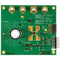
SPIO-4/NOPB National Semiconductor, SPIO-4/NOPB Datasheet - Page 6

SPIO-4/NOPB
Manufacturer Part Number
SPIO-4/NOPB
Description
BOARD INTERFACE FOR AFE
Manufacturer
National Semiconductor
Datasheet
1.SPIO-4NOPB.pdf
(26 pages)
Specifications of SPIO-4/NOPB
Main Purpose
Interface, Analog Front End (AFE)
Embedded
Yes, MCU, 32-Bit
Utilized Ic / Part
SAM3U, XC6SLX16
Primary Attributes
USB Powered or External Supply
Secondary Attributes
GUI, I2C, SPI, USB Interfaces
Accessory Type
Digital Interface Board
Msl
MSL 1 - Unlimited
Lead Free Status / RoHS Status
Lead free / RoHS Compliant
Other names
SPI0-4/NOPB
SPI0-4/NOPB
SPI0-4/NOPB
Available stocks
Company
Part Number
Manufacturer
Quantity
Price
Company:
Part Number:
SPIO-4/NOPB
Manufacturer:
National Semiconductor
Quantity:
135
National Semiconductor
2 System Functionality
2.1 System Block Diagram
2.2 General System Overview
The SPIO-4 board is controlled via the Atmel SAM3U micro-controller that is based on an ARM M3, 32-bit
embedded core. It provides the interface to the computer via a USB interface. The DUT board interfaces
to the SPIO-4 via J6, the GPSI-16/32 connector. The GPSI-16/32 interface provides control, data and
power to the DUT board. The interfaces on the GPSI-32 can be I2C, SPI with multiple-device capability,
and parallel interface. The dedicated I2C interface on the GPSI-16/32 is primarily for control and DUT
identification, while the dedicated SPI interface may be used for control or for data transfer. The I2C
interface is derived from the peripheral of the microcontroller. As there can be a wide variety of SPI
requirements for DUTs, the SPI interface can be provided via a processor peripheral and over the
dedicated SPI lines as shown in this document, or the on-board Xilinx Spartan XC6SLX16 FPGA may be
used. In fact, the FPGA may be used to implement DUT interfaces other than SPI – such as high-speed
I2C for data purposes and parallel data-plus-clock interfaces. A large external SRAM 8Mx16 is connected
to both the processor and the FPGA which is used to provide additional device data storage in case the
microcontroller’s or FPGA’s on-board memory is insufficient.
Power is provided to the system via the USB cable, or external power jack. A switching regulator is used
to produce the 3.3 volt supply required by the microcontroller and GPSI-32 devices. A boost regulator
creates the regulated 5 volt supply required by the devices interfaced to the GPSI-32 connector.
(J10)
Pwr
Ext
SD Card
Connector
(J7)
USB
(J8)
USB
Connector(J1)
5V
Protection
Debug
Input
I2C
USB
8MBx16
PSRAM
(U4)
Connector(J9)
Switching
Regulator
LP3910
Multiple
Supply
(U11)
Debug
1.8V
Figure 2 - SPIO-4 System Block Diagram
DUT3.3V_EN
Micro-Controller
Atmel SAM3U
3.3V
1.2V
(U1)
Static Mem intrfc
12MHZ
NBS0-1
A23-1
D15-0
NCS0
NWR
Xtal
NRD
JTAG
(J2)
NCS2
32kHZ
Xtal
XC6SLX16
Spartan 6
NCS3/FPGA_CFG
Page 6
(U5)
GPIO
DEBUG
IO Voltage
(J4)
DUT3.3V_EN
DUT 3.3V
GPSI A
Regulator
GPSI A
Boost
(U12)
3.3V
Level Shifters
Level Shifters
Filter
GPSI B
>
<
3.3V_DUT
3.3V_DUT
DUT 5V
I2C(SCL)
I2C(SDA)
DUT 3.3V
GPSI A
GPSI A
DUT 5V
VDDIO
Pins 1,3,7,8,16
Pins 5,6,9
Pin 12
Pin 11
Pins 23-30
Pin 15
Pin 13
Pin 14
Connector
GPSI 32
(J6)
www.national.com


