RDK-249 Power Integrations, RDK-249 Datasheet - Page 8
RDK-249
Manufacturer Part Number
RDK-249
Description
KIT REF DESIGN PFS762HG
Manufacturer
Power Integrations
Series
HiperTFS®r
Specifications of RDK-249
Main Purpose
Reference Design, PC Power Supply
Embedded
No
Utilized Ic / Part
TFS762HG
Primary Attributes
12V 25A, 5V 2.9A Outputs, 300 ~ 385 VDC Input
Output Voltage
5 V
Input / Supply Voltage (max)
385 VDC
Input / Supply Voltage (min)
300 VDC
Duty Cycle (max)
50 %
Mounting Style
Through Hole
Output Current
2.9 A
Output Power
14.5 W
Lead Free Status / RoHS Status
Lead free / RoHS Compliant
Secondary Attributes
-
Other names
596-1398


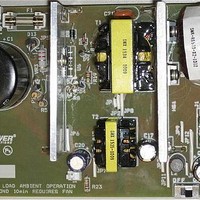
regulated 5.85 V supply. Zener diode VR4 provides a voltage reference for Q1 to regulate
the emitter voltage to 12.4 V for a stable 6 mA into BP pin.
The ENABLE (EN) pin is the feedback pin for the Standby controller section. Prior to the
start-up a resistor R27 connected from EN to BP can be detected to select on of several
internal current limits for Standby section. FEEDBACK (FB) pin resistor R25 can also be
used to select one of three Main current limits at start-up in the same manner as the EN
pin. Four different resistor values can be used for R27 to select one of the four internal
current limit configurations for the Standby section, and three different values for R25 to
select one of the three current limit configurations for the Main section. The circuit
presented here uses R27 (280 k) for a standby I
3.5 A.
The FB pin provides feedback for the Main converter. An increase in current sink from FB
pin to ground will lead to a reduction in the operating duty cycle.
Diode D9 is used to provide the initial power for the bootstrap charging C3 and C6 during
start-up. During this time the high-side MOSFET HS pin is briefly pulled to Source for 12
ms. Once the main converter begins switching after the initial 12 ms bootstrap delay,
diode D5 is used to provide the internal nominal power for the high-side section from the
Main transformer support winding, pins 1 and 2. The normal voltage on C6 during normal
operation is shunt regulated to approximately 12 V. It is necessary to insure at all times a
minimum of 13 V on C3.
Resistors R18, R19, and R36 are used to translate the maximum available OFF time
reset voltage into a current for the R pin and compare with the L pin current to compute
the maximum allowable duty cycle to prevent saturation and also determines the
maximum allowable duty factor as a function of peak on-time flux.
The LINE-SENSE (L) pin provides an input bulk voltage line-sense function. This
information is used by the under-voltage and over-voltage detection circuits for both the
Main and standby sections. This pin can also be pulled down to SOURCE to implement a
remote-ON/OFF of both the Standby and Main supplies simultaneously. Resistors R12,
R13, and R35 are used to translate the input voltage into a current for L pin.
4.3 Output Rectification
For the Standby section, output rectification is provided by diode D11. A low ESR
capacitor, C17, provides filtering with low ripple. Inductor L2 and capacitor C15 form a
post-filter to further reduce switching ripple and noise in the output.
For the Main section diode D7 rectifies during Main on-time and diode D6 is the catch
diode to provide a current discharge path for the output inductor, L1, during the Main off-
time. Inductor L1 together with capacitors C10 and C11 form an output filter out switching
output ripple and noise.
Power Integrations, Inc.
Tel: +1 408 414 9200 Fax: +1 408 414 9201
www.powerint.com
LIM
of 650 mA and R25 for a Main I
Page 8 of 48
LIM
of
Related parts for RDK-249
Image
Part Number
Description
Manufacturer
Datasheet
Request
R

Part Number:
Description:
KIT REF DESIGN TOP HX FOR TOP258
Manufacturer:
Power Integrations
Datasheet:

Part Number:
Description:
KIT REF DESIGN LINKSWITCH 2
Manufacturer:
Power Integrations
Datasheet:

Part Number:
Description:
KIT REF DESIGN 1.2W PS TN FAMILY
Manufacturer:
Power Integrations
Datasheet:

Part Number:
Description:
KIT REF DESIGN 36-72W MOTOR DRVR
Manufacturer:
Power Integrations
Datasheet:

Part Number:
Description:
KIT REF DESIGN FOR LNK457D
Manufacturer:
Power Integrations
Datasheet:

Part Number:
Description:
REFERENCE DESIGN LINKSWITCH-PH
Manufacturer:
Power Integrations
Datasheet:

Part Number:
Description:
Specifications: Manufacturer: Power Integrations ; Output Voltage: 380 VDC ; Input / Supply Voltage (Max): 264 VAC ; Input / Supply Voltage (Min): 90 VAC ; Mounting Style: Through Hole ; Output Current: 0.913 A ; Output Power: 347 W
Manufacturer:
Power Integrations, Inc.

Part Number:
Description:
Power Management Modules & Development Tools TOPSwitch-JX REF. DESIGN KIT
Manufacturer:
Power Integrations
Datasheet:
Part Number:
Description:
Power Management IC Development Tools REF DESIGN RDR-292 PFF LED STREET LIGHT
Manufacturer:
Power Integrations

Part Number:
Description:
KIT REF DESIGN FOR LNK403EG
Manufacturer:
Power Integrations
Datasheet:

Part Number:
Description:
KIT REF DESIGN FOR LNK406EG
Manufacturer:
Power Integrations
Datasheet:

Part Number:
Description:
KIT REF DESIGN DG CAPZERO
Manufacturer:
Power Integrations
Datasheet:

Part Number:
Description:
KIT REF DESIGN LINKSWITCH-CV
Manufacturer:
Power Integrations
Datasheet:
Part Number:
Description:
Specifications: Family: Eval Boards - DC/DC & AC/DC (Off-Line) SMPS ; Series: HiperLCS™ ; Main Purpose: DC/DC, Step Down ; Outputs and Type: 1, Isolated ; Power - Output: 150W ; Voltage - Output: 24V ; Current - Output: 6.25A ; Voltage - Input:
Manufacturer:
Power Integrations, Inc.
Datasheet:

Part Number:
Description:
KIT REFERENCE DESIGN W/TN376PN
Manufacturer:
Power Integrations
Datasheet: