RDK-249 Power Integrations, RDK-249 Datasheet - Page 23
RDK-249
Manufacturer Part Number
RDK-249
Description
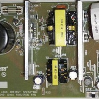
KIT REF DESIGN PFS762HG
Manufacturer
Power Integrations
Series
HiperTFS®r
Specifications of RDK-249
Main Purpose
Reference Design, PC Power Supply
Embedded
No
Utilized Ic / Part
TFS762HG
Primary Attributes
12V 25A, 5V 2.9A Outputs, 300 ~ 385 VDC Input
Output Voltage
5 V
Input / Supply Voltage (max)
385 VDC
Input / Supply Voltage (min)
300 VDC
Duty Cycle (max)
50 %
Mounting Style
Through Hole
Output Current
2.9 A
Output Power
14.5 W
Lead Free Status / RoHS Status
Lead free / RoHS Compliant
Secondary Attributes
-
Other names
596-1398


Control Functions
Switching Frequency
- PC Main
Frequency Jitter
Modulation Rate
Remote-ON Main
BYPASS Pin
Remote-ON Current
BYPASS Pin Remote-
OFF Current Hysteresis
BYPASS Pin Latching
Shutdown Threshold
Main/Standby Remote-
ON Delay
Main/Standby Remote-
OFF Delay
Main/Standby Remote-
OFF Long Time Period
Soft-Start
High-Side Start-Up
Charge Time
Main Current Limit
at Start-Up
Soft-Start Period
www.powerint.com
Thermal Resistance
High-Side MOSFET (θ
Absolute Maximum Ratings
DRAIN Voltage High-Side MOSFET .......................-0.3 V to 530 V
DRAIN Peak Current High-Side: TFS757 ................... 3.1 (5.9)
DRAIN Voltage Low-Side MOSFET .................... -0.3 V to 725 V
DRAIN Peak Current Low-Side: TFS757 ................... 3.1 (5.9)
DRAIN Voltage Standby MOSFET ...................... -0.3 V to 725 V
DRAIN Peak Current Standby MOSFET ................ 1.20 (2.25)
Enable (EN) Pin Voltage ..................... ....................... -0.3 V to 9 V
Enable (EN) Pin Current ................. ................................. 100 mA
Feedback (FB) Pin Voltage ................. ...................... -0.3 V to 9 V
Parameter
JC
) TFS757, TFS758 .................... 15 °C/W
TFS759, TFS760 .................... 14 °C/W
TFS761, TFS762 .................... 13 °C/W
TFS763, TFS764 .................... 12 °C/W
Symbol
t
R(PERIOD)
I
I
I
I
t
f
f
BP(OFF)
t
BP(ON)
t
LIM(SS)
(1,5)
BP(SD)
M(MA)
R(OFF)
S(MA)
R(ON)
D(CH)
TFS758 ...................4.5 (8.4)
TFS759 ...................5.0 (9.3)
TFS760 ................. 5.7 (10.7)
TFS761 ..................6.1 (11.4)
TFS762 ..................6.4 (12.1)
TFS763 ................. 7.2 (13.4)
TFS764 ................. 8.3 (15.5)
TFS758 ...................4.5 (8.4)
TFS759 ...................5.0 (9.3)
TFS760 ................. 5.7 (10.7)
TFS761 ..................6.1 (11.4)
TFS762 ..................6.4 (12.1)
TFS763 ................. 7.2 (13.4)
TFS764................. 8.3 (15.5)
SOURCE = 0 V; T
T
J
(Unless Otherwise Specified)
= 25 °C
Conditions
V
See Note A
EN
= Open
4
4
4
4
4
4
4
4
4
4
4
4
4
4
4
4
4
J
A
A
A
A
A
A
A
A
A
A
A
A
A
A
A
A
A
= 0 °C to 100 °C
Peak-to-Peak Jitter
Low-Side MOSFET (θ
Notes:
1. All voltages referenced to SOURCE, T
Feedback (FB) Current ................... ................................. 100 mA
Line Sense (L) Pin Voltage ............................................-0.3 V to 9 V
Line Sense (L) Pin Current ............................................ .......100 ma
Reset (R) Pin Voltage ..................... ........................... -0.3 V to 9 V
Reset (R) Pin Current ..................................... .................... 100 mA
Bypass Supply (BP) Pin Voltage ............................... -0.3 V to 9 V
Bypass Supply (BP) Pin Current ................................... ..... 100 mA
High Side (VDDH) Supply Pin Voltage ................. -0.3 V to 13.4 V
High Side (VDDH) Supply Pin Current ..................................50 mA
Storage Temperature ............................................ -65 °C to 150 °C
Operating Junction Temperature
Lead Temperature
Notes:
1. All voltages referenced to SOURCE, T
2. Normally limited by internal circuitry.
3. 1/16 in. (1.59 mm) from case for 5 seconds.
4. The higher peak DRAIN current is allowed while the DRAIN
5. Maximum ratings specified may be applied one at a time,
Average
voltage is simultaneously less than 400 V.
without causing permanent damage to the product.
Exposure to Absolute Rating conditions for extended periods
of time may affect product reliability.
(3)
................................................................. 260 °C
JC
Min
3.2
62
13
) ................................................1 °C/W
(2)
15.5
Typ
250
115
TFS757-764HG
3.8
1.1
2.5
2.5
.......................-40 °C to 150 °C
66
80
14
4
A
J
= 25 °C.
= 25 °C.
Max
17.5
4.4
70
12
Units
kHz
mA
mA
mA
Hz
ms
ms
ms
ms
ms
Rev. C 02/11
%
23
Related parts for RDK-249
Image
Part Number
Description
Manufacturer
Datasheet
Request
R

Part Number:
Description:
KIT REF DESIGN TOP HX FOR TOP258
Manufacturer:
Power Integrations
Datasheet:

Part Number:
Description:
KIT REF DESIGN LINKSWITCH 2
Manufacturer:
Power Integrations
Datasheet:

Part Number:
Description:
KIT REF DESIGN 1.2W PS TN FAMILY
Manufacturer:
Power Integrations
Datasheet:

Part Number:
Description:
KIT REF DESIGN 36-72W MOTOR DRVR
Manufacturer:
Power Integrations
Datasheet:

Part Number:
Description:
KIT REF DESIGN FOR LNK457D
Manufacturer:
Power Integrations
Datasheet:

Part Number:
Description:
REFERENCE DESIGN LINKSWITCH-PH
Manufacturer:
Power Integrations
Datasheet:

Part Number:
Description:
Specifications: Manufacturer: Power Integrations ; Output Voltage: 380 VDC ; Input / Supply Voltage (Max): 264 VAC ; Input / Supply Voltage (Min): 90 VAC ; Mounting Style: Through Hole ; Output Current: 0.913 A ; Output Power: 347 W
Manufacturer:
Power Integrations, Inc.

Part Number:
Description:
Power Management Modules & Development Tools TOPSwitch-JX REF. DESIGN KIT
Manufacturer:
Power Integrations
Datasheet:
Part Number:
Description:
Power Management IC Development Tools REF DESIGN RDR-292 PFF LED STREET LIGHT
Manufacturer:
Power Integrations

Part Number:
Description:
KIT REF DESIGN FOR LNK403EG
Manufacturer:
Power Integrations
Datasheet:

Part Number:
Description:
KIT REF DESIGN FOR LNK406EG
Manufacturer:
Power Integrations
Datasheet:

Part Number:
Description:
KIT REF DESIGN DG CAPZERO
Manufacturer:
Power Integrations
Datasheet:

Part Number:
Description:
KIT REF DESIGN LINKSWITCH-CV
Manufacturer:
Power Integrations
Datasheet:
Part Number:
Description:
Specifications: Family: Eval Boards - DC/DC & AC/DC (Off-Line) SMPS ; Series: HiperLCS™ ; Main Purpose: DC/DC, Step Down ; Outputs and Type: 1, Isolated ; Power - Output: 150W ; Voltage - Output: 24V ; Current - Output: 6.25A ; Voltage - Input:
Manufacturer:
Power Integrations, Inc.
Datasheet:

Part Number:
Description:
KIT REFERENCE DESIGN W/TN376PN
Manufacturer:
Power Integrations
Datasheet: