EVAL-ADF4360-5EBZ1 Analog Devices Inc, EVAL-ADF4360-5EBZ1 Datasheet - Page 9
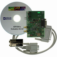
EVAL-ADF4360-5EBZ1
Manufacturer Part Number
EVAL-ADF4360-5EBZ1
Description
BOARD EVALUATION FOR ADF4360-5
Manufacturer
Analog Devices Inc
Datasheet
1.ADF4360-5BCPZ.pdf
(24 pages)
Specifications of EVAL-ADF4360-5EBZ1
Main Purpose
Timing, Frequency Synthesizer
Embedded
No
Utilized Ic / Part
ADF4360-5
Primary Attributes
Single Integer-N PLL with VCO
Secondary Attributes
1.3GHz, 200kHz PFD
Lead Free Status / RoHS Status
Lead free / RoHS Compliant


CIRCUIT DESCRIPTION
REFERENCE INPUT SECTION
The reference input stage is shown in Figure 10. SW1 and SW2
are normally closed switches. SW3 is normally open. When
power-down is initiated, SW3 is closed, and SW1 and SW2 are
opened. This ensures that there is no loading of the REF
on power-down.
PRESCALER (P/P + 1)
The dual-modulus prescaler (P/P + 1), along with the A and B
counters, enables the large division ratio, N , to be realized
(N = BP + A). The dual-modulus prescaler, operating at CML
levels, takes the clock from the VCO and divides it down to a
manageable frequency for the CMOS A and B counters. The
prescaler is programmable. It can be set in software to 8/9,
16/17, or 32/33 and is based on a synchronous 4/5 core. There is
a minimum divide ratio possible for fully contiguous output
frequencies; this minimum is determined by P, the prescaler
value, and is given by (P
A AND B COUNTERS
The A and B CMOS counters combine with the dual-modulus
prescaler to allow a wide range division ratio in the PLL feed-
back counter. The counters are specified to work when the pre-
scaler output is 300 MHz or less. Thus, with a VCO frequency of
2.5 GHz, a prescaler value of 16/17 is valid, but a value of 8/9 is
not valid.
Pulse Swallow Function
The A and B counters, in conjunction with the dual-modulus
prescaler, make it possible to generate output frequencies that
are spaced only by the reference frequency divided by R. The
VCO frequency equation is
where:
f
P is the preset modulus of the dual-modulus prescaler (8/9,
16/17, and so on).
B is the preset divide ratio of the binary 13-bit counter (3 to 8191).
A is the preset divide ratio of the binary 5-bit swallow counter (0 to 31).
f
VCO
REFIN
is the output frequency of the VCO.
is the external reference frequency oscillator.
f
VCO
[ =
REF
(
P
IN
×
NC
B
POWER-DOWN
Figure 10. Reference Input Stage
)
SW1
+
CONTROL
A
NO
× ]
2
NC
− P).
f
SW3
REFIN
SW2
100kΩ
/
R
BUFFER
TO R COUNTER
IN
pin
Rev. A | Page 9 of 24
R COUNTER
The 14-bit R counter allows the input reference frequency to
be divided down to produce the reference clock to the phase
frequency detector (PFD). Division ratios from 1 to 16,383 are
allowed.
PFD AND CHARGE PUMP
The PFD takes inputs from the R counter and N counter
(N = BP + A) and produces an output proportional to the phase
and frequency difference between them. Figure 12 is a simpli-
fied schematic. The PFD includes a programmable delay ele-
ment that controls the width of the antibacklash pulse. This
pulse ensures that there is no dead zone in the PFD transfer
function and minimizes phase noise and reference spurs. Two
bits in the R counter latch, ABP2 and ABP1, control the width of
the pulse (see Table 9).
CP OUTPUT
R DIVIDER
N DIVIDER
R DIVIDER
N DIVIDER
FROM VCO
HI
HI
Figure 12. PFD Simplified Schematic and Timing (In Lock)
D1
D2
CLR1
CLR2
U1
U2
N = BP + A
N DIVIDER
MODULUS
CONTROL
Q1
Q2
Figure 11. A and B Counters
PROGRAMMABLE
ABP1
PRESCALER
UP
DOWN
P/P+1
DELAY
ABP2
LOAD
LOAD
COUNTER
COUNTER
13-BIT B
5-BIT A
U3
ADF4360-5
CPGND
V
P
TO PFD
CHARGE
PUMP
CP
Related parts for EVAL-ADF4360-5EBZ1
Image
Part Number
Description
Manufacturer
Datasheet
Request
R

Part Number:
Description:
±1.7g Dual-Axis IMEMS Accelerometer Evaluation Board
Manufacturer:
Analog Devices Inc
Datasheet:

Part Number:
Description:
Inertial Sensor Evaluation System
Manufacturer:
Analog Devices Inc
Datasheet:
Part Number:
Description:
Manufacturer:
Analog Devices Inc
Datasheet:
Part Number:
Description:
Manufacturer:
Analog Devices Inc
Datasheet:
Part Number:
Description:
Manufacturer:
Analog Devices Inc
Datasheet:
Part Number:
Description:
Manufacturer:
Analog Devices Inc
Datasheet:
Part Number:
Description:
Manufacturer:
Analog Devices Inc
Datasheet:
Part Number:
Description:
Manufacturer:
Analog Devices Inc
Datasheet:
Part Number:
Description:
Manufacturer:
Analog Devices Inc
Datasheet:
Part Number:
Description:
Manufacturer:
Analog Devices Inc
Datasheet:
Part Number:
Description:
Manufacturer:
Analog Devices Inc
Datasheet:
Part Number:
Description:
Manufacturer:
Analog Devices Inc
Datasheet:
Part Number:
Description:
Manufacturer:
Analog Devices Inc
Datasheet: