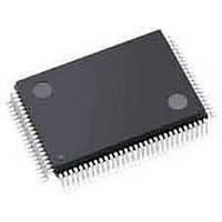
AGLN250V2-VQG100 Actel, AGLN250V2-VQG100 Datasheet - Page 26

AGLN250V2-VQG100
Manufacturer Part Number
AGLN250V2-VQG100
Description
FPGA - Field Programmable Gate Array 250K System Gates IGLOO nano
Manufacturer
Actel
Datasheet
1.AGLN030V5-ZUCG81.pdf
(140 pages)
Specifications of AGLN250V2-VQG100
Processor Series
AGLN250
Core
IP Core
Number Of Macrocells
2048
Maximum Operating Frequency
250 MHz
Number Of Programmable I/os
68
Data Ram Size
36 Kbit
Supply Voltage (max)
1.5 V
Supply Current
34 uA
Maximum Operating Temperature
+ 70 C
Minimum Operating Temperature
- 20 C
Development Tools By Supplier
AGLN-Nano-Kit, AGLN-Z-Nano-Kit, AGL-Dev-Kit-SCS, Silicon-Explorer II, Silicon-Sculptor 3, SI-EX-TCA, FLASHPRO 4, FlashPro 3, FLASHPRO LITE
Mounting Style
SMD/SMT
Supply Voltage (min)
1.2 V
Number Of Gates
250 K
Package / Case
VQFP-100
Lead Free Status / RoHS Status
Lead free / RoHS Compliant
Available stocks
Company
Part Number
Manufacturer
Quantity
Price
Company:
Part Number:
AGLN250V2-VQG100
Manufacturer:
Actel
Quantity:
135
Company:
Part Number:
AGLN250V2-VQG100
Manufacturer:
Microsemi SoC
Quantity:
10 000
Company:
Part Number:
AGLN250V2-VQG100I
Manufacturer:
Microsemi SoC
Quantity:
10 000
IGLOO nano DC and Switching Characteristics
2- 12
Power Calculation Methodology
This section describes a simplified method to estimate power consumption of an application. For more
accurate and detailed power estimations, use the SmartPower tool in Actel Libero IDE software.
The power calculation methodology described below uses the following variables:
Methodology
Total Power Consumption—P
Total Static Power Consumption—P
Total Dynamic Power Consumption—P
Global Clock Contribution—P
Sequential Cells Contribution—P
•
•
•
•
•
•
•
•
P
P
P
P
P
TOTAL
STAT
DYN
CLOCK
S-CELL
The number of PLLs as well as the number and the frequency of each output clock generated
The number of combinatorial and sequential cells used in the design
The internal clock frequencies
The number and the standard of I/O pins used in the design
The number of RAM blocks used in the design
Toggle rates of I/O pins as well as VersaTiles—guidelines are provided in
page
Enable rates of output buffers—guidelines are provided for typical applications in
page
Read rate and write rate to the memory—guidelines are provided for typical applications in
Table 2-20 on page
design.
P
P
N
N
Table 2-19 on page
N
Table 2-19 on page
F
N
PAC1, PAC2, PAC3, and PAC4 are device-dependent.
N
multi-tile sequential cell is used, it should be accounted for as 1.
α
page
F
= P
= (PDC1 or PDC2 or PDC3) + N
CLK
CLK
STAT
DYN
BANKS
SPINE
ROW
S-CELL
S-CELL
1
= P
= (PAC1 + N
= N
2-14.
2-14.
CLOCK
is the toggle rate of VersaTile outputs—guidelines are provided in
STAT
is the global clock signal frequency.
is the global clock signal frequency.
2-14.
is the total dynamic power consumption.
S-CELL
is the total static power consumption.
is the number of VersaTile rows used in the design—guidelines are provided in
is the number of global spines used in the user design—guidelines are provided in
is the number of I/O banks powered in the design.
is the number of VersaTiles used as sequential modules in the design.
is the number of VersaTiles used as sequential modules in the design. When a
+ P
+ P
* (PAC5 +
DYN
S-CELL
SPINE
2-14. The calculation should be repeated for each clock domain defined in the
2-14.
2-14.
+ P
* PAC2 + N
α
C-CELL
1
TOTAL
CLOCK
/ 2 * PAC6) * F
S-CELL
+ P
ROW
BANKS
STAT
R ev i sio n 1 1
NET
DYN
* PAC3 + N
+ P
* PDC5
CLK
INPUTS
S-CELL
+ P
OUTPUTS
* PAC4) * F
+ P
MEMORY
CLK
+ P
PLL
Table 2-19 on
Table 2-19 on
Table 2-20 on


