ADIS16204BCCZ Analog Devices Inc, ADIS16204BCCZ Datasheet - Page 17
ADIS16204BCCZ
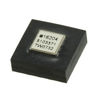
Manufacturer Part Number
ADIS16204BCCZ
Description
IC ACCEL DIGITAL HI-G 16-LGA
Manufacturer
Analog Devices Inc
Datasheet
1.ADIS16204PCBZ.pdf
(24 pages)
Specifications of ADIS16204BCCZ
Acceleration Range
±37g, 70g
Axis
X, Y
Sensitivity
17.125 LSB/mg, 8.407 LSB/mg
Voltage - Supply
3 V ~ 3.6 V
Output Type
Digital
Bandwidth
400Hz
Interface
SPI
Mounting Type
Surface Mount
Package / Case
16-LGA
No. Of Axes
2
Sensor Case Style
LGA
No. Of Pins
16
Supply Voltage Range
3V To 3.6V
Operating Temperature Range
-40°C To +105°C
Svhc
No SVHC (18-Jun-2010)
Family Name
ADIS16204
Package Type
LGA
Operating Supply Voltage (min)
3V
Operating Supply Voltage (typ)
3.3V
Operating Supply Voltage (max)
3.6V
Operating Temperature (min)
-40C
Operating Temperature (max)
105C
Operating Temperature Classification
Industrial
Product Depth (mm)
8mm
Product Height (mm)
5.2mm
Product Length (mm)
8mm
Mounting
Surface Mount
Pin Count
16
Interface Type
SPI
Sensitivity Per Axis
17.125mg / LSB
Rohs Compliant
Yes
Lead Free Status / RoHS Status
Lead free / RoHS Compliant
For Use With
ADIS16204/PCBZ - BOARD EVAL FOR ADIS16204/PCB
Lead Free Status / Rohs Status
Compliant
Available stocks
Company
Part Number
Manufacturer
Quantity
Price
Company:

Part Number:
ADIS16204BCCZ
Manufacturer:
ST
Quantity:
390


General-Purpose I/O
The ADIS16204 provides two general-purpose pins that
enable digital I/O control using the SPI. The GPIO_CTRL
control register establishes the configuration of these pins
and handles the SPI-to-pin controls. Each pin provides the
flexibility of both input (read) and output (write) operations.
For example, writing a 0x0202 to this register establishes Line 1
as an input and Line 2 as an output that is in a 1 state. Writing
0x0000 to this register establishes both lines as inputs. When
one (or both) of these lines is configured as an input, reading
the assigned bit (Bit 8 and/or Bit 9) provides access to the input
on this input pin.
The digital I/O lines are also available for data-ready and alarm/
error indications. In the event of conflict, the following priority
structure governs the digital I/O configuration:
1.
2.
3.
Table 21. GPIO_CTRL Register Definition
Address
0x33, 0x32
Table 22. GPIO_CTRL Bit Descriptions
Bit
15:10
9
8
7:2
1
0
STATUS AND DIAGNOSTICS
The ADIS16204 provides a number of status and diagnostic
functions. Table 23 provides a summary of these functions,
along with their appropriate control registers.
Table 23. Status and Diagnostic Functions
Function
Data-ready I/O indicator
Self-test, mechanical check for MEMS sensor
Software check for error conditions
Flash memory endurance
Data-Ready I/O Indicator
The data-ready function provides an indication of new output
data. The MSC_CTRL register provides the opportunity to
configure either of the general-purpose I/O pins (DIO1 and DIO2)
GPIO_CTRL
MSC_CTRL
ALM_CTRL
Description
Not used
General-purpose I/O Line 2 polarity
General-purpose I/O Line 1 polarity
Not used
General-purpose I/O Line 2, data direction control
General-purpose I/O Line 1, data direction control
1 = high, 0 = low
1 = high, 0 = low
1 = output, 0 = input
1 = output, 0 = input
Default
0x0000
Format
N/A
Register
MSC_CTRL
MSC_CTRL
STATUS
ENDURANCE
Access
R/W
Rev. B | Page 17 of 24
as a data-ready indicator signal. When configured as a data ready
indicator, the duty cycle is 20% (±10% tolerance).
Self-Test
The MSC_CTRL register also provides a self-test function
that verifies the mechanical integrity of the MEMS sensor. A
self-test exercises the mechanical structure and signal condi-
tioning circuit: from sensor element to data out. The internal
test provides a simple, two-step process for checking the MEMS
sensor: (1) start the process by writing a 1 to Bit 8 in the
MSC_CTRL register, (2) wait 35 ms, and (3) check the result
by reading Bit 5 of the STATUS register.
The device is configured to perform a self-test at power on.
Writing a 1 to Bit 10 of the MSC_CTRL register disables this
function for future start-up sequences, reducing the start-up
time. For reference, the result of the electrostatic deflection
of each axis is available by reading the XACCL_OUT and/or
YACCL_OUT registers. As an additional indicator of self-test,
the new data bit is not active while in this mode.
Table 24. MSC_CTRL Register Definition
Address
0x35, 0x34
Table 25. MSC_CTRL Bit Descriptions
Bit
15:12
11
10
9
8
7:3
2
1
0
Flash Memory Endurance
The ENDURANCE register maintains a running count of writes to
the flash memory. This provides a convenient tool for managing
the reliability of the on-chip memory. Once it reaches its maxi-
mum value of 32,767, it wraps around to zero and starts over.
Table 26. ENDURANCE Register Definition
Address
0x01, 0x00
Description
Not used
Store capture to flash after capture buffer fills up
Self-test at power-on
Not used
Self-test enable (temporary, bit is volatile)
Not used
Data-ready enable
Data-ready polarity
Data-ready line select
1 = enabled, 0 = disabled
1 = disabled, 0 = enabled
1 = enabled, 0 = disabled
1 = enabled, 0 = disabled
1 = active high, 0 = active low
1 = DIO2, 0 = DIO1
Default
0x0000
Default
N/A
Binary
Format
N/A
Format
ADIS16204
Access
R/W
Access
R only
Related parts for ADIS16204BCCZ
Image
Part Number
Description
Manufacturer
Datasheet
Request
R

Part Number:
Description:
±1.7g Dual-Axis IMEMS Accelerometer Evaluation Board
Manufacturer:
Analog Devices Inc
Datasheet:

Part Number:
Description:
Inertial Sensor Evaluation System
Manufacturer:
Analog Devices Inc
Datasheet:
Part Number:
Description:
Manufacturer:
Analog Devices Inc
Datasheet:
Part Number:
Description:
Manufacturer:
Analog Devices Inc
Datasheet:
Part Number:
Description:
Manufacturer:
Analog Devices Inc
Datasheet:
Part Number:
Description:
Manufacturer:
Analog Devices Inc
Datasheet:
Part Number:
Description:
Manufacturer:
Analog Devices Inc
Datasheet:
Part Number:
Description:
Manufacturer:
Analog Devices Inc
Datasheet:
Part Number:
Description:
Manufacturer:
Analog Devices Inc
Datasheet:
Part Number:
Description:
Manufacturer:
Analog Devices Inc
Datasheet:
Part Number:
Description:
Manufacturer:
Analog Devices Inc
Datasheet:
Part Number:
Description:
Manufacturer:
Analog Devices Inc
Datasheet:
Part Number:
Description:
Manufacturer:
Analog Devices Inc
Datasheet: