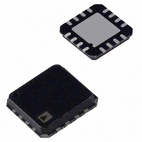
AD8305ACPZ-RL7 Analog Devices Inc, AD8305ACPZ-RL7 Datasheet - Page 17

AD8305ACPZ-RL7
Manufacturer Part Number
AD8305ACPZ-RL7
Description
IC, LOGARITHMIC AMP, 20mV, LFCSP-16
Manufacturer
Analog Devices Inc
Type
Logarithmic Converterr
Datasheet
1.AD8305ACPZ-RL7.pdf
(24 pages)
Specifications of AD8305ACPZ-RL7
No. Of Amplifiers
1
Dynamic Range, Decades
5
Scale Factor V / Decade
0.2
Supply Voltage Range
3V To 12V
Amplifier Case Style
LFCSP
Supply Current
5.4mA
Input Offset Voltage
20mV
Design Resources
Interfacing ADL5315 to Translinear Logarithmic Amplifier (CN0056) Interfacing ADL5317 High Side Current Mirror to a Translinear Logarithmic Amplifier in an Avalanche Photodiode Power Detector
Applications
Fiber Optics
Mounting Type
Surface Mount
Package / Case
16-LFCSP
Rohs Compliant
Yes
Number Of Channels
1
Number Of Elements
3
Power Supply Requirement
Single/Dual
Single Supply Voltage (typ)
5V
Dual Supply Voltage (typ)
±3/±5V
Power Dissipation
500mW
Rail/rail I/o Type
Rail to Rail Output
Single Supply Voltage (min)
3V
Single Supply Voltage (max)
12V
Dual Supply Voltage (min)
±1.5V
Dual Supply Voltage (max)
±6V
Operating Temp Range
-40C to 85C
Operating Temperature Classification
Industrial
Mounting
Surface Mount
Pin Count
16
Package Type
LFCSP EP
Lead Free Status / RoHS Status
Lead free / RoHS Compliant
Lead Free Status / RoHS Status
Lead free / RoHS Compliant, Lead free / RoHS Compliant
Other names
AD8305ACPZ-RL7
LOG-RATIO APPLICATIONS
It is often desirable to determine the ratio of two currents, for
example, in absorbance measurements. These are commonly
used to assess the attenuation of a passive optical component,
such as an optical filter or variable optical attenuator. In these
situations, a reference detector is used to measure the incident
power entering the component. The exiting power is then
measured using a second detector and the ratio is calculated to
determine the attenuation factor. Because the AD8305 is
fundamentally a ratiometric device, having nearly identical
logging systems for both numerator and denominator (I
I
Figure 38 illustrates the AD8305 log-ratio capabilities in optical
absorbance measurements. Here a reference detector diode is
used to provide the reference current, I
optical reference power level. A second detector measures the
transmitted signal power, proportional to I
calculates the logarithm of the ratio of these two currents, as
shown in Equation 11, and which is reformulated in power
terms in Equation 12. Both of these equations include the
internal factor of 10,000 introduced by the output offset applied
to V
Equation 4 is preferred, VRDZ should be grounded to remove
the offset. As already noted, the use of a negative supply at Pin
VNEG allows both V
ground, and also allow the input pins INPT and IREF to be set
to ground potential. Therefore, the AD8305 may also be used to
determine the log ratio of two voltages.
Figure 38 also illustrates how a second order Sallen-Key low-
pass filter can be realized using two external capacitors and one
resistor. Here, the corner frequency is set to 1 kHz and the filter
Q is chosen to provide an optimally flat (overshoot-free) pulse
response. To scale this frequency either up or down, simply
scale the capacitors by the appropriate factor. Note that one of
the resistors needed to realize this filter is the output resistance
REF
, respectively), it can greatly simplify such measurements.
LOG
via pin VRDZ. If the true (nonoffset) log ratio shown in
LOG
and the buffer output to swing below
REF
, proportional to the
PD
. The AD8305
PD
and
Rev. B | Page 17 of 24
of 4.55 kΩ present at Pin VLOG. While this does not ratio
exactly to the external resistor, which may slightly alter the Q of
the filter, the effect on pulse response is be negligible for most
purposes. Note that the gain of the buffer (×2.5) is an integral
part of this illustrative filter design; in general, the filter may be
redesigned for other closed-loop gains.
The transfer characteristics can be expressed in terms of optical
power. If we assume that the two detectors have equal
responsivities, the relationship is
Using the identity log
attenuation as −10 × log
characteristic can be written as
where α = −10 × log
Figure 39 illustrates the linear-in-dB relationship between the
absorbance and the output of the circuit in Figure 38.
V
V
2.5
2.0
1.5
1.0
0.5
OUT
OUT
0
0
Figure 39. Example of an Absorbance Transfer Function
= 0.5 V log
= 2 − 50 mV/dB × α
5
10
10
10
10
(P
(10
15
(AB) = log
SIG
10
4
(P
ATTENUATION (dB)
/P
× P
20
SIG
REF
/P
SIG
)
REF
/P
25
10
REF
), the overall transfer
A + log
)
30
35
10
B and defining the
40
45
AD8305
50
(11)
(12)


