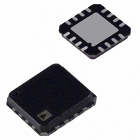
AD8305ACPZ-RL7 Analog Devices Inc, AD8305ACPZ-RL7 Datasheet - Page 21

AD8305ACPZ-RL7
Manufacturer Part Number
AD8305ACPZ-RL7
Description
IC, LOGARITHMIC AMP, 20mV, LFCSP-16
Manufacturer
Analog Devices Inc
Type
Logarithmic Converterr
Datasheet
1.AD8305ACPZ-RL7.pdf
(24 pages)
Specifications of AD8305ACPZ-RL7
No. Of Amplifiers
1
Dynamic Range, Decades
5
Scale Factor V / Decade
0.2
Supply Voltage Range
3V To 12V
Amplifier Case Style
LFCSP
Supply Current
5.4mA
Input Offset Voltage
20mV
Design Resources
Interfacing ADL5315 to Translinear Logarithmic Amplifier (CN0056) Interfacing ADL5317 High Side Current Mirror to a Translinear Logarithmic Amplifier in an Avalanche Photodiode Power Detector
Applications
Fiber Optics
Mounting Type
Surface Mount
Package / Case
16-LFCSP
Rohs Compliant
Yes
Number Of Channels
1
Number Of Elements
3
Power Supply Requirement
Single/Dual
Single Supply Voltage (typ)
5V
Dual Supply Voltage (typ)
±3/±5V
Power Dissipation
500mW
Rail/rail I/o Type
Rail to Rail Output
Single Supply Voltage (min)
3V
Single Supply Voltage (max)
12V
Dual Supply Voltage (min)
±1.5V
Dual Supply Voltage (max)
±6V
Operating Temp Range
-40C to 85C
Operating Temperature Classification
Industrial
Mounting
Surface Mount
Pin Count
16
Package Type
LFCSP EP
Lead Free Status / RoHS Status
Lead free / RoHS Compliant
Lead Free Status / RoHS Status
Lead free / RoHS Compliant, Lead free / RoHS Compliant
Other names
AD8305ACPZ-RL7
EVALUATION BOARD
An evaluation board is available for the AD8305, the schematic for which is shown in Figure 49. It can be configured for a wide variety of
experiments. The buffer gain is factory-set to unity, providing a slope of 200 mV/decade, and the intercept is set to 1 nA. Table 4 describes
the various configuration options.
Table 4. Evaluation Board Configuration Options
Component
P1
P2, R8, R9, R10,
R11, R17, R18
R2, R3, R4, R6,
R14, C2, C7, C9,
C10
R1, R7, R19, R20
R12, R15, C3, C4,
C5, C6
C11
R13, R16, C1, C8
IREF, INPT, PD,
LK1, R5
J1
Function
Supply interface. Provides access to supply pins, VNEG, COMM, and VPOS.
Monitor Interface. By adding 0 Ω resistors to R8, R9, R10, R11, R17, and R18, the
VRDZ, VREF, VSUM, VOUT, and VLOG pin voltages can be monitored using a high
impedance probe.
Buffer amplifier/output interface. The logarithmic slope of the AD8305 can be
altered using the buffer’s gain-setting resistors, R2 and R3. R4, R14, and C2 allow
variation in the buffer loading. R6, C7, C9, and C10 are provided for a variety of
filtering applications.
Intercept adjustment. The voltage dropped across resistor R1 determines the
intercept reference current, nominally set to 10 μA using a 200 kΩ 1% resistor. R7
and R19 can be used to adjust the output-offset voltage at the VLOG output.
Supply Decoupling.
VSUM decoupling capacitor.
Input compensation. Provides essential HF compensation at the input pins, INPT
and IREF.
Input interface. The test board is configured to accept a current through the SMA
connector labeled INPT. An SC-style packaged photodiode can be used in place
of the INPT SMA for optical interfacing. By removing R1 and adding a 0 Ω short
for R5, a second current can be applied to the IREF input (also SMA) for evaluating
the AD8305 in log-ratio applications.
SC-Style Photodiode. Allows for direct mounting of SC style photodiodes.
Rev. B | Page 21 of 24
Default Condition
P1 = installed
P2 = Not installed
R8 = R9 = R10 = Open (size 0603)
R17 = R18 = Open (size 0603)
R2 = R6 = 0 Ω (size 0603)
R3 = R4 = open (size 0603)
R11 = R14 = 0 Ω (size 0603)
C2 = C7 = open (size 0603)
C9 = C10 = open (size 0603)
VLOG = VOUT = installed
R1 = 200 kΩ (size 0603)
R7 = R19 = 0 Ω (size 0603)
R20 = open (size 0603)
C3 = C4 = 0.01 μF
(size 0603)
C5 = C6 = 0.1 μF (size 0603)
R12 = R15 = 0 Ω (size 0603)
C11 = 1 nF (size 0603)
R13 = R16 = 1 kΩ (size 0603)
C1 = C8 = 1 nF (size 0603)
IREF = INPT = installed
PD = not installed
LK1 = installed
R5 = open (size 0603)
J1 = not installed
AD8305


