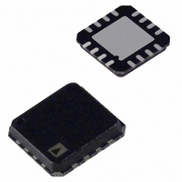
AD8330ACPZ-R2 Analog Devices Inc, AD8330ACPZ-R2 Datasheet - Page 28

AD8330ACPZ-R2
Manufacturer Part Number
AD8330ACPZ-R2
Description
IC, VAR GAIN AMP, 150MHZ, 2DB, LFCSP-16
Manufacturer
Analog Devices Inc
Datasheet
1.AD8330-EVALZ.pdf
(32 pages)
Specifications of AD8330ACPZ-R2
No. Of Amplifiers
1
Bandwidth
150MHz
Gain Accuracy
2dB
Rail To Rail I/o Type
Rail Rail Outputs
No. Of Channels
1
Supply Voltage Range
2.7V To 6V
Amplifier Case Style
LFCSP
Amplifier Type
Variable Gain
Number Of Circuits
1
Output Type
Differential, Rail-to-Rail
Slew Rate
1500 V/µs
-3db Bandwidth
150MHz
Current - Input Bias
100nA
Current - Supply
20mA
Voltage - Supply, Single/dual (±)
2.7 V ~ 6 V
Operating Temperature
-40°C ~ 85°C
Mounting Type
Surface Mount
Package / Case
16-LFCSP
Rohs Compliant
Yes
Lead Free Status / RoHS Status
Lead free / RoHS Compliant
For Use With
AD8330-EVALZ - BOARD EVAL FOR AD8330
Current - Output / Channel
-
Gain Bandwidth Product
-
Voltage - Input Offset
-
Lead Free Status / RoHS Status
Lead free / RoHS Compliant, Lead free / RoHS Compliant
AD8330
EVALUATION BOARD
GENERAL DESCRIPTION
The AD8330-EVALZ is an easy-to-use accessory that enables a
hands-on evaluation of the
(VGA). It includes test pins for connections to all of the functional
device inputs. Figure 69 is a full size photograph of the board.
Figure 69. Photograph of the AD8330 Evaluation Board
IN
–5V
49.9Ω
R2
AD8330
+
0.1µF
C18
C17
10µF
10V
AD8131
variable gain amplifier
24.9Ω
0.1µF
10µF
10nF
10V
C16
C15
R1
C1
C20
0.1µF
+
+5V
8
2
1
3
6
A1
4
5
VDBS
C14
10nF
0.1µF
0.1µF
C3
C5
GAIN_SLOPE
Figure 70. Schematic Diagram
0.1µF
IN_TEST
C6
OFST
Rev. E | Page 28 of 32
DOWN
+5V
FILTER_OFFSET
R4
0Ω
ENBL
0.1µF
C2
UP
CMGN
1
2
3
4
5
6
7
8
FLTR
OFST
ENBL
VPSI
INHI
INLO
MODE
VDBS
CMGN
BASIC OPERATION
The input SMA connector IN is terminated with a 49.9 Ω
resistor (see Figure 70). For convenience, the board includes an
AD8131
ended signal source to the differential input of the AD8330. If
desired, the AD8131 can be removed and the AD8330 can be
driven at one of its inputs from a single-ended source.
The AD8330 output is observed at the SMA connectors OUT_HI
and OUT_LO or by using the 2-pin header OUT_HI/ OUT_LO
adjacent to the device.
The AD8330 requires only a +5 V power supply; however, because
of the AD8131 buffer bipolar power supply requirements, ±5 V
supplies are required to power the board. The current required
for the board is approximately 40 mA from the +5 V supply and
10 mA from the −5 V supply.
AD8330
DUT1
C13
1nF
COMM
CMOP
VMAG
VPOS
CNTR
VPSO
OPLO
high speed differential amplifier to convert a single-
OPHI
1kΩ
R3
11
10
9
13
12
14
16
15
C12
0.1µF
C19
0.1µF
C11
0.1µF
C9
12pF
C8
12pF
+5V
0.1µF
C7
+5V
GND1 GND2 GND3 GND4
OUT_TEST
CNTR
0.1µF
0.1µF
C10
C4
VMAG
OUT_HI
OUT_ LO


