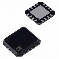
AD8330ACPZ-R2 Analog Devices Inc, AD8330ACPZ-R2 Datasheet - Page 8

AD8330ACPZ-R2
Manufacturer Part Number
AD8330ACPZ-R2
Description
IC, VAR GAIN AMP, 150MHZ, 2DB, LFCSP-16
Manufacturer
Analog Devices Inc
Datasheet
1.AD8330-EVALZ.pdf
(32 pages)
Specifications of AD8330ACPZ-R2
No. Of Amplifiers
1
Bandwidth
150MHz
Gain Accuracy
2dB
Rail To Rail I/o Type
Rail Rail Outputs
No. Of Channels
1
Supply Voltage Range
2.7V To 6V
Amplifier Case Style
LFCSP
Amplifier Type
Variable Gain
Number Of Circuits
1
Output Type
Differential, Rail-to-Rail
Slew Rate
1500 V/µs
-3db Bandwidth
150MHz
Current - Input Bias
100nA
Current - Supply
20mA
Voltage - Supply, Single/dual (±)
2.7 V ~ 6 V
Operating Temperature
-40°C ~ 85°C
Mounting Type
Surface Mount
Package / Case
16-LFCSP
Rohs Compliant
Yes
Lead Free Status / RoHS Status
Lead free / RoHS Compliant
For Use With
AD8330-EVALZ - BOARD EVAL FOR AD8330
Current - Output / Channel
-
Gain Bandwidth Product
-
Voltage - Input Offset
-
Lead Free Status / RoHS Status
Lead free / RoHS Compliant, Lead free / RoHS Compliant
AD8330
Figure 12. Differential Output Offset vs. V
–10
–20
–30
–40
10
–1
–2
–3
–4
–5
–6
–7
50
40
30
20
10
100k
8
6
4
2
0
0
100k
0
Figure 10. Frequency Response for Various Values of V
0
V
DBS
= 0.1V
0.2
Figure 11. Group Delay vs. Frequency
V
MAG
0.4
1M
1M
for a Representative Part
= 4.8V
1.52V
0.48V
0.15V
0.048V
0.015V
0.6
FREQUENCY (Hz)
FREQUENCY (Hz)
V
DBS
V
= 0.75 V
DBS
0.8
10M
(V)
10M
1.0
DBS
T = +25°C
for Three Temperatures,
1.2
T = +85°C
100M
T = –40°C
100M
1.4
MAG
500M
300M
1.6
,
Rev. E | Page 8 of 32
Figure 14. Output Balance Error vs. Frequency for a Representative Part
–10
–20
–30
–40
–50
–60
–70
–80
–90
200
190
180
170
160
150
140
130
120
110
100
10
25
20
15
10
100k
100k
0
5
0
1048 UNITS
ENABLE MODE
Figure 13. Differential Input Offset Histogram
Figure 15. Output Impedance vs. Frequency
1
DIFFERENTIAL OFFSET (mV)
M
1M
FREQUENCY (Hz)
FREQUENCY (Hz)
1
0
M
10M
100M
100M
3
0
0
M


