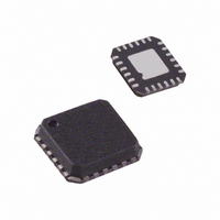
ADF4252BCPZ Analog Devices Inc, ADF4252BCPZ Datasheet - Page 12

ADF4252BCPZ
Manufacturer Part Number
ADF4252BCPZ
Description
IC, FREQUENCY SYNTHESIZER, 3GHZ LFCSP-24
Manufacturer
Analog Devices Inc
Type
Clock/Frequency Synthesizer (RF/IF), Fractional N, Integer Nr
Datasheet
1.ADF4252BCPZ.pdf
(28 pages)
Specifications of ADF4252BCPZ
Pll Type
Frequency Synthesis
Frequency
3GHz
Supply Current
13mA
Supply Voltage Range
2.7V To 3.3V
Digital Ic Case Style
LFCSP
No. Of Pins
24
Operating Temperature Range
-40°C To +85°C
Pll
Yes
Input
CMOS
Output
Clock
Number Of Circuits
1
Ratio - Input:output
3:2
Differential - Input:output
Yes/No
Frequency - Max
3GHz
Divider/multiplier
Yes/No
Voltage - Supply
2.7 V ~ 3.3 V
Operating Temperature
-40°C ~ 85°C
Mounting Type
Surface Mount
Package / Case
24-LFCSP
Frequency-max
3GHz
Rohs Compliant
Yes
Lead Free Status / RoHS Status
Lead free / RoHS Compliant
For Use With
EVAL-ADF4252EBZ2 - BOARD EVAL ADF4252 NO VCO/FILTER
Lead Free Status / RoHS Status
Lead free / RoHS Compliant, Lead free / RoHS Compliant
Available stocks
Company
Part Number
Manufacturer
Quantity
Price
Part Number:
ADF4252BCPZ
Manufacturer:
ADI/亚德诺
Quantity:
20 000
Company:
Part Number:
ADF4252BCPZ-R7
Manufacturer:
AD
Quantity:
2 143
ADF4252
Phase Frequency Detector (PFD) and Charge Pump
The PFD takes inputs from the R counter and N counter and
produces an output proportional to the phase and frequency
difference between them. Figure 6 is a simplified schematic. The
antibacklash pulse. This pulse ensures that there is no dead zone
in the PFD transfer function and minimizes phase noise and
reference spurs.
MUXOUT and Lock Detect
The output multiplexer on the ADF4252 allows the user to
access various internal points on the chip. The state of MUXOUT
is controlled by M4, M3, M2, and M1 in the master register.
Table I shows the full truth table. Figure 7 shows the MUXOUT
section in block diagram format.
IF/RF ANALOG LOCK DETECT
RF/IF DIGITAL LOCK DETECT
RF ANALOG LOCK DETECT
IF ANALOG LOCK DETECT
RF DIGITAL LOCK DETECT
IF DIGITAL LOCK DETECT
RF R DIVIDER OUTPUT
RF N DIVIDER OUTPUT
THREE STATE OUTPUT
IF R DIVIDER OUTPUT
IF N DIVIDER OUTPUT
+IN
–IN
HI
HI
Figure 6. PFD Simplified Schematic
LOGIC HIGH
LOGIC HIGH
LOGIC LOW
LOGIC LOW
Figure 7. MUXOUT Circuit
D1
D2
CLR1
CLR2
U1
U2
Q1
Q2
ELEMENT
DELAY
UP
DOWN
MUX
U3
CONTROL
CHARGE
PUMP
D
DV
GND
DD
CP
MUXOUT
–12–
Lock Detect
MUXOUT can be programmed for two types of lock detect: digital
and analog. Digital is active high. The N-channel open-drain
analog lock detect should be operated with an external pull-up
resistor of 10 kΩ nominal. When lock has been detected, this
output will be high with narrow low going pulses.
Input Shift Register
Data is clocked in on each rising edge of CLK. The data is
clocked in MSB first. Data is transferred from the input register
to one of seven latches on the rising edge of LE. The destination
latch is determined by the state of the three control bits (C2, C1,
and C0) in the shift register. These are the three LSBs: DB2,
DB1, and DB0, as shown in Figure 1. The truth table for these
bits is shown in Table I. Table II summarizes how the registers
are programmed.
C2
0
0
0
0
1
1
1
C1
0
0
1
1
0
0
1
Table I. Control Bit Truth Table
C0
0
1
0
1
0
1
0
Data Latch
RF N Divider Reg
RF R Divider Reg
RF Control Reg
Master Reg
IF N Divider Reg
IF R Divider Reg
IF Control Reg
REV. B


