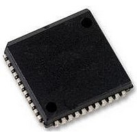
SC16C2552BIA44 NXP Semiconductors, SC16C2552BIA44 Datasheet - Page 21

SC16C2552BIA44
Manufacturer Part Number
SC16C2552BIA44
Description
UART, 2 CH, 16BYTE FIFO, 16C2552
Manufacturer
NXP Semiconductors
Datasheet
1.SC16C2552BIA44.pdf
(38 pages)
Specifications of SC16C2552BIA44
No. Of Channels
2
Data Rate
5Mbps
Supply Voltage Range
2.25V To 5.5V
Operating Temperature Range
-40°C To +85°C
Digital Ic Case Style
PLCC
No. Of Pins
44
Svhc
No SVHC (18-Jun-2010)
Operating
RoHS Compliant
Uart Features
Independent Transmit & Receive UART Control, Multi-Function Output, Modem Control Functions
Rohs Compliant
Yes
Available stocks
Company
Part Number
Manufacturer
Quantity
Price
Part Number:
SC16C2552BIA44
Manufacturer:
NXP/恩智浦
Quantity:
20 000
Company:
Part Number:
SC16C2552BIA44,529
Manufacturer:
NXP Semiconductors
Quantity:
10 000
NXP Semiconductors
SC16C2552B_3
Product data sheet
7.10 Alternate Function Register (AFR)
7.9 Scratchpad Register (SPR)
The SC16C2552B provides a temporary data register to store 8 bits of user information.
This is a read/write register used to select specific modes of MF operation and to allow
both UART register’s sets to be written concurrently.
Table 19.
Table 20.
Bit
7:3
2:1
0
AFR[2]
0
0
1
1
Symbol
AFR[7:3]
AFR[2:1]
AFR[0]
Alternate Function Register bit description
MFA, MFB function selection
AFR[1]
0
1
0
1
5 V, 3.3 V and 2.5 V dual UART, 5 Mbit/s (max.), with 16-byte FIFOs
Description
Not used. All are initialized to logic 0.
Selects a signal function for output on the MFA, MFB pins. These signal
functions are described as: OP2 (interrupt enable), BAUDOUT, or RXRDY.
Only one signal function can be selected at a time. See
When this bit is set, CPU can write concurrently to the same register in both
UARTs. This function is intended to reduce the dual UART initialization time.
It can be used by CPU when both channels are initialized to the same state.
The external CPU can set or clear this bit by accessing either register set.
When this bit is set, the Channel Select pin, CHSEL, still selects the channel
to be accessed during read operation. Setting or clearing this bit has no
effect on read operations. The user should ensure that LCR[7] of both
channels are in the same state before executing a concurrent write to the
registers at address 0, 1, or 2.
Rev. 03 — 12 February 2009
logic 0 = no concurrent write (normal default condition)
logic 1 = register set A and B are written concurrently with a single external
CPU I/O write operation.
MF function
OP2
BAUDOUT
RXRDY
reserved
SC16C2552B
Table
© NXP B.V. 2009. All rights reserved.
20.
21 of 38


