VNC1L FTDI, VNC1L Datasheet - Page 6
VNC1L
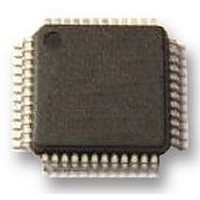
Manufacturer Part Number
VNC1L
Description
IC, USB HOST CONTROLLER, LQFP-48
Manufacturer
FTDI
Datasheet
1.VNC1L.pdf
(17 pages)
Specifications of VNC1L
Usb Type
Host Controller
Usb Version
2.0
No. Of Ports
2
Supply Voltage Range
3V To 3.6V
Operating Temperature Range
0°C To +70°C
Digital Ic Case Style
LQFP
No. Of Pins
48
Termination Type
SMD
Filter Terminals
SMD
Rohs Compliant
Yes
Lead Free Status / RoHS Status
Lead free / RoHS Compliant
Available stocks
Company
Part Number
Manufacturer
Quantity
Price
Company:

Part Number:
VNC1L-1A(VDPSFUL)
Manufacturer:
FUTURETE
Quantity:
750
Company:
Part Number:
VNC1L-1A-REEL
Manufacturer:
TI
Quantity:
3 485
Part Number:
VNC1L-1A-REEL
Manufacturer:
FTDI
Quantity:
20 000


Table 1 - Pin �ut Description
Vinculum VNC1L Embedded USB Host Controller I.C. Datasheet Version 0.96
Pin No.
USB Interface Group
2�
26
28
29
Power and Ground Group
1, 2�, 27, 39
2
3
6
17, 30, �0
Miscellaneous Signal Group
�
�
7
8
9
10
Data and Control Bus Signals
11
12
13
1�
1�
16
18
19
20
21
22
23
31
32
33
3�
3�
36
37
38
�1
2.2 48 Lead LQFP Package Signal Descriptions
Name
USB1DP
USB1D�
USB2DP
USB2D�
�ND
VCC
AVCC
A�ND
VCCI�
XTIN
XT�UT
PLLFLTR
TEST
RESET#
PR��#
BDBUS0
BDBUS1
BDBUS2
BDBUS3
BDBUS�
BDBUS�
BDBUS6
BDBUS7
BCBUS0
BCBUS1
BCBUS2
BCBUS3
ADBUS0
ADBUS1
ADBUS2
ADBUS3
ADBUS�
ADBUS�
ADBUS6
ADBUS7
ACBUS0
Type Description
I/�
I/�
I/�
I/�
PWR
PWR
PWR
PWR
PWR
Input
�utput
Input
Input
Input
Input
I/�
I/�
I/�
I/�
I/�
I/�
I/�
I/�
I/�
I/�
I/�
I/�
I/�
I/�
I/�
I/�
I/�
I/�
I/�
I/�
I/�
USB host / slave port 1 - USB Data Signal Plus with integrated pull up / pull down resistor.
USB host / slave port 1 - USB Data Signal �inus with integrated pull up / pull down resistor.
USB host / slave port 2 - USB Data Signal Plus with integrated pull up / pull down resistor.
USB host / slave port 2 - USB Data Signal �inus with integrated pull up / pull down resistor.
Device ground supply pins
3.3V supply to the device core.
+3.3V supply to the internal cloc�� multiplier. This pin requires a 100 nF decoupling capacitor.
Device analog ground supply for internal cloc�� multiplier
+3.3V supply to the ADBUS, ACBUS, BDBUS and BCBUS Interface pins �11...16, 18...23, 31...38, �1...�8).
Input to 12�H�� �scillator Cell. Connect 12 �H�� crystal across pins � and �, with suitable loading capacitors
to �ND. This pin can also be driven by an e��ternal 12 �H�� cloc�� signal. Note that the switching threshold of
this pin is VCC/2, so if driving from an e��ternal source, the source must be driving at �V C��S level, or a.c.
coupled to centre around VCC/2.
�utput from 12�H�� �scillator Cell. Connect 12 �H�� crystal across pins � and �, with suitable loading
capacitors to �ND. XT�UT stops oscillating during USB suspend, so ta��e care using this signal to cloc��
e��ternal logic.
External PLL filter circuit input� RC filter circuit must be fitted on this pin�
Puts the device into I.C. test mode. �ust be tied to �ND for normal operation.
Can be used by an e��ternal device to reset the VNC1L. This pin can be used in combination with PR��#
and the U�RT inter�ace to program firmware into the VNC1L� I� not required pull up to VCC via a 1�� kΩ
resistor.*
This pin is used in combination with the RESET# pin and the U�RT inter�ace to program firmware into the
VNC1L.*
�V safe bidirectional data / control bus, BD bit 0
�V safe bidirectional data / control bus, BD bit 1
�V safe bidirectional data / control bus, BD bit 2
�V safe bidirectional data / control bus, BD bit 3
�V safe bidirectional data / control bus, BD bit �
�V safe bidirectional data / control bus, BD bit �
�V safe bidirectional data / control bus, BD bit 6
�V safe bidirectional data / control bus, BD bit 7
�V safe bidirectional data / control bus, BC bit 0
�V safe bidirectional data / control bus, BC bit 1
�V safe bidirectional data / control bus, BC bit 2
�V safe bidirectional data / control bus, BC bit 3
�V safe bidirectional data / control bus, AD bit 0
�V safe bidirectional data / control bus, AD bit 1
�V safe bidirectional data / control bus, AD bit 2
�V safe bidirectional data / control bus, AD bit 3
�V safe bidirectional data / control bus, AD bit �
�V safe bidirectional data / control bus, AD bit �
�V safe bidirectional data / control bus, AD bit 6
�V safe bidirectional data / control bus, AD bit 7
�V safe bidirectional data / control bus, AC bit 0
Interface �ode
UART Inter-
face
PS2Cl��1**
PS2Data1**
PS2Cl��2**
PS2Data2**
TXD
RXD
RTS#
CTS#
DTR#
DSR#
DCD#
RI#
TXDEN#
© Future Technology Devices Intl Ltd. 2006-2007
Parallel FIF�
Interface
PS2Cl��1**
PS2Data1**
PS2Cl��2**
PS2Data2**
D0
D1
D2
D3
D�
D�
D6
D7
RXF#
SPI Slave
Interface
PS2Cl��1**
PS2Data1** PortBC1
PS2Cl��2**
PS2Data2** PortBC3
SCLK
SDI
SD�
CS
I/� Port
PortBD0
PortBD1
PortBD2
PortBD3
PortBD�
PortBD�
PortBD6
PortBD7
PortBC0
PortBC2
PortAD0
PortAD1
PortAD2
PortAD3
PortAD�
PortAD�
PortAD6
PortAD7
PortAC0
Related parts for VNC1L
Image
Part Number
Description
Manufacturer
Datasheet
Request
R

Part Number:
Description:
Interface Modules & Development Tools USB to Serial UART MiniB Dev Mod FT232R
Manufacturer:
FTDI
Datasheet:

Part Number:
Description:
BOARD, EVALUATION, EU PSU
Manufacturer:
FTDI
Datasheet:
Part Number:
Description:
BOARD, EVALUATION, UK PSU
Manufacturer:
FTDI
Datasheet:
Part Number:
Description:
BOARD, EVALUATION, US PSU
Manufacturer:
FTDI
Datasheet:
Part Number:
Description:
Specifications: Manufacturer: FTDI ; Product Category: USB Interface IC ; RoHS: Details ; Operating Supply Voltage: 3 V to 5.25 V ; Supply Current: 25 mA ; Maximum Operating Temperature: + 70 C ; Mounting Style: SMD/SMT ; Package / Case: QFN-32
Manufacturer:
FTDI
Part Number:
Description:
integr. usb2.0/uart lqfp32 rohs ftdi reel c1k...
Manufacturer:
FTDI
Datasheet:
Part Number:
Description:
Interface Development Tools USB to UART Breakout Board
Manufacturer:
FTDI
Datasheet:

Part Number:
Description:
IC USB TO SERIAL UART 32-QFN
Manufacturer:
FTDI, Future Technology Devices International Ltd

Part Number:
Description:
USB Interface IC USB to Serial UART Enhanced IC SSOP-28
Manufacturer:
FTDI
Datasheet:

Part Number:
Description:
IC, USB UART INTERFACE, SSOP-28
Manufacturer:
FTDI
Datasheet:

Part Number:
Description:
IC, USB UART INTERFACE, QFN-32
Manufacturer:
FTDI
Datasheet:
Part Number:
Description:
IC, USB FIFO INTERFACE, SSOP-28
Manufacturer:
FTDI
Datasheet:
Part Number:
Description:
MODULE, USB, 4 PORT, FT4232H BASED
Manufacturer:
FTDI
Datasheet:
Part Number:
Description:
357-036-542-201 CARDEDGE 36POS DL .156 BLK LOPRO
Manufacturer:
FTDI
Datasheet:
Part Number:
Description:
357-036-542-201 CARDEDGE 36POS DL .156 BLK LOPRO
Manufacturer:
FTDI
Datasheet: