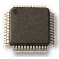
VNC1L FTDI, VNC1L Datasheet - Page 9

VNC1L
Manufacturer Part Number
VNC1L
Description
IC, USB HOST CONTROLLER, LQFP-48
Manufacturer
FTDI
Datasheet
1.VNC1L.pdf
(17 pages)
Specifications of VNC1L
Usb Type
Host Controller
Usb Version
2.0
No. Of Ports
2
Supply Voltage Range
3V To 3.6V
Operating Temperature Range
0°C To +70°C
Digital Ic Case Style
LQFP
No. Of Pins
48
Termination Type
SMD
Filter Terminals
SMD
Rohs Compliant
Yes
Lead Free Status / RoHS Status
Lead free / RoHS Compliant
Available stocks
Company
Part Number
Manufacturer
Quantity
Price
Company:
Part Number:
VNC1L-1A(VDPSFUL)
Manufacturer:
FUTURETE
Quantity:
750
Company:
Part Number:
VNC1L-1A-REEL
Manufacturer:
TI
Quantity:
3 485
Part Number:
VNC1L-1A-REEL
Manufacturer:
FTDI
Quantity:
20 000
Table 8 - Data and Control Bus Signal �ode �ptions - SPI Interface
Figure 6 - SPI Slave Data Read Cycle
From Start - SPI CS must be held high for the entire read cycle, and must be ta��en low for at least one cloc�� period
a�ter the read is completed� The first bit on SPI Data In is the R�W bit - inputting a ‘1’ here allows data to be read �rom
the chip� The next bit is the address bit�� �DD�� which is used to indicate whether the data register (‘��’) or the status
register (‘1’) is read �rom� During the SPI read cycle a byte o� data will start being output on SPI Data Out on the next
clock cycle a�ter the address bit�� MSB first� ��ter the data has been clocked out o� the chip�� the status o� SPI Data
Out should be checked to see i� the data read is new data� � ‘��’ level here on SPI Data Out means that the data read
is new data� � ‘1’ indicates that the data read is old data�� and the read cycle should be repeated to get new data�
Remember that CS must be held low for at least one cloc�� period before being ta��en high again to continue with the
ne��t read or write cycle.
Figure 7 - SPI Slave Data Write Cycle
From Start - SPI CS must be held high for the entire write cycle, and must be ta��en low for at least one cloc�� period
a�ter the write is completed� The first bit on SPI Data In is the R�W bit - inputting a ‘��’ here allows data to be written
to the chip� The next bit is the address bit�� �DD�� which is used to indicate whether the data register (‘��’) or the status
Vinculum VNC1L Embedded USB Host Controller I.C. Datasheet Version 0.96
SPI Data �ut
SPI Data �ut
Pin No.
31
32
33
3�
SPI Data In
SPI Data In
SPI CS
SPI CS
SPICLK
SPICLK
2.5 SPI Interface Signal Descriptions and Timing Diagrams
Name
SCLK
SDI
SD�
CS
Type
Input
Input
�utput
Input
1
1
R/W ADD
0
R/W ADD
1
Description
SPI Cloc�� input, 12�H�� ma��imum.
SPI Serial Data Input
SPI Serial Data �utput
SPI Chip Select Input
0
0
D7
D7
D6
D6
D�
D�
D�
D3
D�
D2
D3
© Future Technology Devices Intl Ltd. 2006-2007
D1
D2
D0
D1
D0


