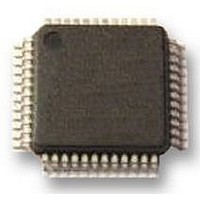
VNC2-48L1B FTDI, VNC2-48L1B Datasheet - Page 53

VNC2-48L1B
Manufacturer Part Number
VNC2-48L1B
Description
CONTROLLER, USB, VINCULUM II, 48LQFP
Manufacturer
FTDI
Datasheet
1.VNC2-32Q1B-REEL.pdf
(90 pages)
Specifications of VNC2-48L1B
Usb Type
Host Controller
Usb Version
2.0
Data Rate
12Mbps
No. Of Ports
2
Supply Voltage Range
1.62V To 1.98V, 2.97V To 3.63V
Operating Temperature Range
-40°C To +85°C
Digital Ic Case
RoHS Compliant
Available stocks
Company
Part Number
Manufacturer
Quantity
Price
Company:
Part Number:
VNC2-48L1B-REEL
Manufacturer:
TELIT
Quantity:
879
Company:
Part Number:
VNC2-48L1B-REEL
Manufacturer:
FTDI, Future Technology Devices International Ltd
Quantity:
10 000
Company:
Part Number:
VNC2-48L1B-TRAY
Manufacturer:
RENESAS
Quantity:
101
Company:
Part Number:
VNC2-48L1B-TRAY
Manufacturer:
FTDI, Future Technology Devices International Ltd
Quantity:
10 000
Table 22 SPI Master Data Read Status Bit
Figure 6-17 SPI Master Data Read (VNC2 Slave Mode)
The status bit is only valid until the next rising edge of SCLK after the last data bit.
During the Data Read operation the SS signal must not be de-asserted.
The transfer completes after 12 clock cycles and the next transfer can begin when MOSI and SS are high
during the rising edge of SCLK.
6.3.6.3 SPI Master Data Write Transaction in VNC1L legacy mode
During an SPI master Data Write operation the Start and Setup sequence is sent by the SPI master to
VNC2, see Figure 6-18. This is followed by the SPI master transmitting each bit of the data to be written
to VNC2. The VNC2 then responds with a status bit on MISO on the rising edge of the next clock cycle.
The SPI master must read the status bit at the end of each write transaction to determine if the data was
written successfully to VNC2 Receive Buffer. The Data Write status bit is defined in Table 23.The status
bit is only valid until the next rising edge of SCLK after the last data bit.
If the status bit indicates Accept then the byte transmitted has been added to VNC2 Receive Buffer. If it
shows Reject then the Receive Buffer is full and the byte of data transmitted in the current transaction
should be re-transmitted by the SPI master to VNC2.
Any application should poll VNC2 Receive Buffer by retrying the Data Write operation until the data is
accepted.
Table 23 SPI Master Data Write Status Bit
Status Bit
Status Bit
0
1
0
1
Meaning
New Data
Old Data
Accept
Reject
Copyright © 2010 Future Technology Devices International Limited
Data in current transaction is valid data.
Byte removed from Transmit Buffer.
This same data has been read in a previous read cycle.
Repeat the read cycle until New Data is received.
VINCULUM-II EMBEDDED DUAL USB HOST CONTROLLER IC Datasheet
Data from the current transaction was accepted and added to the
Write data was not accepted.
Meaning
Retry the same write cycle.
Receive Buffer
Document No.: FT_000138
Clearance No.: FTDI#
Version -
143
1.2
53


