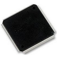
LFXP6C-5TN144C LATTICE SEMICONDUCTOR, LFXP6C-5TN144C Datasheet - Page 18

LFXP6C-5TN144C
Manufacturer Part Number
LFXP6C-5TN144C
Description
FPGA, 1.8V FLASH, INSTANT ON, SMD
Manufacturer
LATTICE SEMICONDUCTOR
Series
LatticeXPr
Datasheet
1.LFXP3C-3QN208C.pdf
(130 pages)
Specifications of LFXP6C-5TN144C
No. Of Logic Blocks
720
No. Of Macrocells
3000
Family Type
LatticeXP
No. Of Speed Grades
5
No. Of I/o's
100
Clock Management
PLL
Core Supply Voltage Range
1.71V To 3.465V
Lead Free Status / RoHS Status
Lead free / RoHS Compliant
Available stocks
Company
Part Number
Manufacturer
Quantity
Price
Company:
Part Number:
LFXP6C-5TN144C
Manufacturer:
LATTICE
Quantity:
2 291
Company:
Part Number:
LFXP6C-5TN144C
Manufacturer:
Lattice
Quantity:
60
Company:
Part Number:
LFXP6C-5TN144C
Manufacturer:
Lattice Semiconductor Corporation
Quantity:
10 000
Company:
Part Number:
LFXP6C-5TN144C-4I
Manufacturer:
LATTICE
Quantity:
2 291
Lattice Semiconductor
Figure 2-17. PIC Diagram
In the LatticeXP family, seven PIOs or four (3.5) PICs are grouped together to provide two LVDS differential pairs,
one PIC pair and one single I/O, as shown in Figure 2-18.
Two adjacent PIOs can be joined to provide a differential I/O pair (labeled as “T” and “C”). The PAD Labels “T” and
“C” distinguish the two PIOs. Only the PIO pairs on the left and right edges of the device can be configured as
LVDS transmit/receive pairs.
One of every 14 PIOs (a group of 8 PICs) contains a delay element to facilitate the generation of DQS signals as
shown in Figure 2-19. The DQS signal feeds the DQS bus which spans the set of 13 PIOs (8 PICs). The DQS sig-
nal from the bus is used to strobe the DDR data from the memory into input register blocks. This interface is
designed for memories that support one DQS strobe per eight bits of data.
The exact DQS pins are shown in a dual function in the Logic Signal Connections table in this data sheet. Addi-
tional detail is provided in the Signal Descriptions table in this data sheet.
DDRCLKPOL
ONEG1
ONEG0
OPOS1
OPOS0
IPOS0
IPOS1
GSRN
INDD
INCK
INFF
DQS
CLK
LSR
CE
TD
Control
Muxes
CLKO
CEO
GSR
CLKI
LSR
CEI
2-15
TD
DDRCLK
PIO B
D0
D1
DDRCLK
D0
D1
INDD
INCK
INFF
IPOS0
PIO A
IPOS1
Register Block
Register Block
(2 Flip Flops)
Register Block
(2 Flip Flops)
(5 Flip Flops)
Tristate
Output
Input
IOLD0
IOLT0
DO
DI
LatticeXP Family Data Sheet
Buffer
sysIO
PADB “C”
PADA
Architecture
"T"


