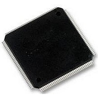
LFXP6C-5TN144C LATTICE SEMICONDUCTOR, LFXP6C-5TN144C Datasheet - Page 27

LFXP6C-5TN144C
Manufacturer Part Number
LFXP6C-5TN144C
Description
FPGA, 1.8V FLASH, INSTANT ON, SMD
Manufacturer
LATTICE SEMICONDUCTOR
Series
LatticeXPr
Datasheet
1.LFXP3C-3QN208C.pdf
(130 pages)
Specifications of LFXP6C-5TN144C
No. Of Logic Blocks
720
No. Of Macrocells
3000
Family Type
LatticeXP
No. Of Speed Grades
5
No. Of I/o's
100
Clock Management
PLL
Core Supply Voltage Range
1.71V To 3.465V
Lead Free Status / RoHS Status
Lead free / RoHS Compliant
Available stocks
Company
Part Number
Manufacturer
Quantity
Price
Company:
Part Number:
LFXP6C-5TN144C
Manufacturer:
LATTICE
Quantity:
2 291
Company:
Part Number:
LFXP6C-5TN144C
Manufacturer:
Lattice
Quantity:
60
Company:
Part Number:
LFXP6C-5TN144C
Manufacturer:
Lattice Semiconductor Corporation
Quantity:
10 000
Company:
Part Number:
LFXP6C-5TN144C-4I
Manufacturer:
LATTICE
Quantity:
2 291
Lattice Semiconductor
Typical I/O Behavior During Power-up
The internal power-on-reset (POR) signal is deactivated when V
After the POR signal is deactivated, the FPGA core logic becomes active. It is the user’s responsibility to ensure
that all other V
I/O banks that are critical to the application. The default configuration of the I/O pins in a blank device is tri-state
with a weak pull-up to VCCIO. The I/O pins will not take on the user configuration until VCC, VCCAUX and VCCIO
have reached satisfactory levels at which time the I/Os will take on the user-configured settings.
The V
fers. In order to simplify system design while providing consistent and predictable I/O behavior, it is recommended
that the I/O buffers be powered-up prior to the FPGA core fabric. V
together with the V
Supported Standards
The LatticeXP sysIO buffer supports both single-ended and differential standards. Single-ended standards can be
further subdivided into LVCMOS, LVTTL and other standards. The buffers support the LVTTL, LVCMOS 1.2, 1.5,
1.8, 2.5 and 3.3V standards. In the LVCMOS and LVTTL modes, the buffer has individually configurable options for
drive strength, bus maintenance (weak pull-up, weak pull-down, or a bus-keeper latch) and open drain. Other sin-
gle-ended standards supported include SSTL and HSTL. Differential standards supported include LVDS, BLVDS,
LVPECL, differential SSTL and differential HSTL. Tables 2-7 and 2-8 show the I/O standards (together with their
supply and reference voltages) supported by the LatticeXP devices. For further information on utilizing the sysIO
buffer to support a variety of standards please see the details of additional technical documentation at the end of
this data sheet.
Table 2-7. Supported Input Standards
CC
and V
Single Ended Interfaces
LVTTL
LVCMOS33
LVCMOS25
LVCMOS18
LVCMOS15
LVCMOS12
PCI
HSTL18 Class I, II
HSTL18 Class III
HSTL15 Class I
HSTL15 Class III
SSTL3 Class I, II
SSTL2 Class I, II
SSTL18 Class I
Differential Interfaces
Differential SSTL18 Class I
Differential SSTL2 Class I, II
Differential SSTL3 Class I, II
Differential HSTL15 Class I, III
Differential HSTL18 Class I, II, III
LVDS, LVPECL
BLVDS
1. When not specified V
2. JTAG inputs do not have a fixed threshold option and always follow V
CCIO
CCAUX
CC
banks are active with valid input logic levels to properly control the output logic states of all the
Input Standard
supply the power to the FPGA core fabric, whereas the V
and V
2
2
2
CCAUX
CCIO
supplies.
can be set anywhere in the valid operating range.
V
REF
2-24
1.08
0.75
1.25
0.9
0.9
1.5
—
—
—
—
—
—
—
0.9
—
—
—
—
—
—
—
(Nom.)
CC
CCIO
and V
CCJ.
supplies should be powered up before or
CCAUX
LatticeXP Family Data Sheet
CCIO
V
have reached satisfactory levels.
CCIO
supplies power to the I/O buf-
1.8
1.5
3.3
1
—
—
—
—
—
—
—
—
—
—
—
—
—
—
—
—
—
—
(Nom.)
Architecture


