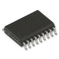
74LV245D NXP Semiconductors, 74LV245D Datasheet - Page 2

74LV245D
Manufacturer Part Number
74LV245D
Description
74LV, SMD, 74LV245, SOIC20, 3.3V
Manufacturer
NXP Semiconductors
Datasheet
1.74LV245D.pdf
(12 pages)
Specifications of 74LV245D
Logic Device Type
Transceiver, Non Inverting
Supply Voltage Range
1V To 5.5V
Logic Case Style
SOIC
No. Of Pins
20
Operating Temperature Range
-40°C To +125°C
Svhc
No SVHC (18-Jun-2010)
Package
RoHS Compliant
Available stocks
Company
Part Number
Manufacturer
Quantity
Price
Company:
Part Number:
74LV245D
Manufacturer:
PHILPS
Quantity:
2 613
Company:
Part Number:
74LV245DB
Manufacturer:
NXP
Quantity:
1 230
Company:
Part Number:
74LV245DB,118
Manufacturer:
NXP
Quantity:
4 641
1. C
Philips Semiconductors
FEATURES
QUICK REFERENCE DATA
GND = 0 V; T
NOTE:
ORDERING INFORMATION
PIN DESCRIPTION
t
C
C
C
20-Pin Plastic DIL
20-Pin Plastic SO
20-Pin Plastic SSOP Type II
20-Pin Plastic TSSOP Type I
1
2, 3, 4, 5,
6, 7, 8, 9
10
18, 17, 16, 15,
14, 13, 12, 11
19
20
1998 Apr 20
PHL
SYMBOL
Wide operating voltage: 1.0 to 5.5 V
Optimized for low voltage applications: 1.0 to 3.6 V
Accepts TTL input levels between V
Typical V
T
Typical V
T
Output capability: bus driver
I
PIN NUMBER
Octal bus transceiver (3-State)
I
I/O
PD
CC
P
f
f
amb
amb
i
o
PD
D
= input frequency in MHz; C
/t
= output frequency in MHz; V
(C
category: MSI
PLH
= C
= 25 C
= 25 C
L
is used to determine the dynamic power dissipation (P
PD
OLP
OHV
V
PACKAGES
amb
CC
Propagation delay
A
Input capacitance
Input/output capacitance
Power dissipation capacitance per buffer
(output ground bounce) < 0.8 V at V
(output V
n
V
2
= 25 C; t
to B
CC
DIR
A
GND
B
OE
V
SYMBOL
2
f
0
0
CC
n
o
; B
) = sum of the outputs.
to A
to B
OH
f
n
i
r
) (C
7
to A
7
= t
undershoot) > 2 V at V
PARAMETER
f
n
Direction
Data inputs/outputs
Ground (0 V)
Data inputs/outputs
Output enable input (active LOW)
Positive supply voltage
2.5 ns
L
L
= output load capacitance in pF;
CC
CC
= supply voltage in V;
V
TEMPERATURE RANGE
CC
= 2.7 V and V
2
–40 C to +125 C
–40 C to +125 C
–40 C to +125 C
–40 C to +125 C
FUNCTION
f
o
) where:
CC
CC
= 3.3 V,
= 3.3 V,
CC
= 3.6 V
C
V
V
V
D
L
CC
CC
I
= GND to V
= 15 pF;
in W)
= 3.3 V
= 3.3 V
OUTSIDE NORTH AMERICA
2
CONDITIONS
H =
L =
X =
Z =
DESCRIPTION
The 74LV245 is a low-voltage Si-gate CMOS device and is pin and
function compatible with 74HC/HCT245.
The 74LV245 is an octal transceiver featuring non-inverting 3-State
bus compatible outputs in both send and receive directions. The
74LV245 features an output enable (OE) input for easy cascading
and a send/receive (DIR) input for direction control. OE controls the
outputs so that the buses are effectively isolated.
CC
FUNCTION TABLE
NOTES:
74LV245 DB
74LV245 PW
, note 1
74LV245 N
74LV245 D
OE
H
L
L
HIGH voltage level
LOW voltage level
don’t care
high impedance OFF-state
INPUTS
DIR
H
X
L
NORTH AMERICA
74LV245PW DH
74LV245 DB
74LV245 N
74LV245 D
TYPICAL
7.0
3.5
10
40
Inputs
A = B
A
Z
INPUTS/OUTPUT
n
Product specification
853–1931 19258
74LV245
PKG. DWG. #
SOT146-1
SOT163-1
SOT339-1
SOT360-1
Inputs
UNIT
B = A
pF
pF
pF
ns
B
Z
n


