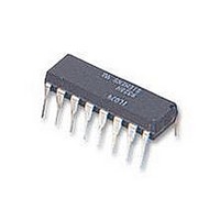
HEF4017BP NXP Semiconductors, HEF4017BP Datasheet - Page 2

HEF4017BP
Manufacturer Part Number
HEF4017BP
Description
IC 5-STAGE JOHNSON DECADE COUNTER, DIP16
Manufacturer
NXP Semiconductors
Datasheet
1.HEF4017BP.pdf
(8 pages)
Specifications of HEF4017BP
Counter Type
Decade, Johnson
Clock Frequency
30MHz
Count Maximum
5
Supply Voltage Range
4.5V To 15.5V
Logic Case Style
DIP
No. Of Pins
16
Operating Temperature Range
-40°C To +70°C
Lead Free Status / RoHS Status
Lead free / RoHS Compliant
Available stocks
Company
Part Number
Manufacturer
Quantity
Price
Company:
Part Number:
HEF4017BP
Manufacturer:
NXP
Quantity:
540
Company:
Part Number:
HEF4017BP
Manufacturer:
PHILIPS
Quantity:
125
Company:
Part Number:
HEF4017BP
Manufacturer:
PHI
Quantity:
6 219
Part Number:
HEF4017BP
Manufacturer:
NXP/恩智浦
Quantity:
20 000
Company:
Part Number:
HEF4017BP,642
Manufacturer:
NXP
Quantity:
16 000
Philips Semiconductors
DESCRIPTION
The HEF4017B is a 5-stage Johnson decade counter with
ten spike-free decoded active HIGH outputs (O
active LOW output from the most significant flip-flop (O
active HIGH and active LOW clock inputs (CP
an overriding asynchronous master reset input (MR).
The counter is advanced by either a LOW to HIGH
transition at CP
transition at CP
table).
When cascading counters, the O
while the counter is in states 5, 6, 7, 8 and 9, can be used
to drive the CP
January 1995
HEF4017BP(N):
HEF4017BD(F):
HEF4017BT(D):
( ): Package Designator North America
5-stage Johnson counter
0
0
1
input of the next counter.
while CP
while CP
Fig.2 Pinning diagram.
16-lead DIL; plastic (SOT38-1)
16-lead DIL; ceramic (cerdip) (SOT74)
16-lead SO; plastic (SOT109-1)
1
0
is LOW or a HIGH to LOW
is HIGH (see also function
5-9
output, which is LOW
0
o
Fig.1 Functional diagram.
, CP
to O
1
9
) and
), an
5-9
),
2
A HIGH on MR resets the counter to zero
(O
clock inputs (CP
Automatic code correction of the counter is provided by an
internal circuit: following any illegal code the counter
returns to a proper counting mode within 11 clock pulses.
Schmitt-trigger action in the clock input makes the circuit
highly tolerant to slower clock rise and fall times.
PINNING
FAMILY DATA, I
See Family Specifications
CP
CP
MR
O
O
o
0
5-9
0
1
= O
to O
5-9
9
= HIGH; O
clock input (LOW to HIGH triggered)
clock input (HIGH to LOW triggered)
master reset input
decoded outputs
carry output (active LOW)
0
DD
, CP
LIMITS category MSI
1
1
).
to O
9
= LOW) independent of the
Product specification
HEF4017B
MSI


