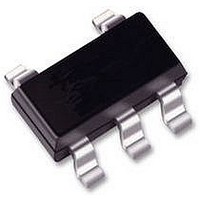
74AHCT1G14GW/T1 NXP Semiconductors, 74AHCT1G14GW/T1 Datasheet - Page 11

74AHCT1G14GW/T1
Manufacturer Part Number
74AHCT1G14GW/T1
Description
74AHCT SINGLE GATE, SMD, 74AHCT1G14
Manufacturer
NXP Semiconductors
Datasheet
1.74AHCT1G14GWT1.pdf
(20 pages)
Specifications of 74AHCT1G14GW/T1
Output Current
8mA
No. Of Inputs
1
Supply Voltage Range
4.5V To 5.5V
Logic Case Style
SOT-353
No. Of Pins
5
Operating Temperature Range
-40°C To +125°C
Svhc
No SVHC
Logic Type
Inverter Gate
Lead Free Status / RoHS Status
Lead free / RoHS Compliant
Philips Semiconductors
2002 Jun 06
handbook, halfpage
handbook, halfpage
Inverting Schmitt trigger
I CC(AV)
Fig.13 Typical AHCT1G14 transfer characteristics;
Fig.14 Average I
( A)
(mA)
I CC
200
150
100
50
8
6
4
2
0
0
0
0
V
devices; linear change of V
0.1V
CC
= 5.5 V.
CC
to 0.9V
CC
2.0
2
for AHC1G Schmitt-trigger
CC
.
4.0
positive-going
negative-going
4
I
edge
V CC (V)
edge
between
V I (V)
MNA036
MNA405
6.0
6
11
APPLICATION INFORMATION
The slow input rise and fall times cause additional power
dissipation, this can be calculated using the following
formula:
P
Average I
transitions, as shown in Figs 14 and 15.
For AHC1G/AHCT1G14 used in relaxation oscillator
circuit, see Fig.16.
Note to the application information:
1. All values given are typical unless otherwise specified.
handbook, halfpage
ad
P
f
t
t
I
i
r
f
CC(AV)
I CC(AV)
Fig.15 Average I
ad
= input frequency (MHz);
= f
= input fall time (ns); 90% to 10%;
= input rise time (ns); 10% to 90%;
( A)
= additional power dissipation ( W);
200
150
100
i
50
0
= average additional supply current ( A).
(t
0
CC
r
devices; linear change of V
0.1V
74AHC1G14; 74AHCT1G14
differs with positive or negative input
I
CC(AV)
CC
to 0.9V
CC
+ t
2
f
for AHCT1G Schmitt-trigger
CC
I
CC(AV)
.
)
positive-going
4
negative-going
V
edge
Product specification
CC
I
V CC (V)
between
edge
where:
MNA058
6


