74HC132D NXP Semiconductors, 74HC132D Datasheet - Page 2
74HC132D
Manufacturer Part Number
74HC132D
Description
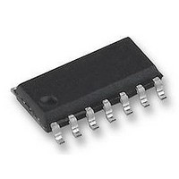
IC, 74HC CMOS, SMD, 74HC132, SOIC14
Manufacturer
NXP Semiconductors
Datasheet
1.74HC132D.pdf
(8 pages)
Specifications of 74HC132D
Output Current
5.2mA
No. Of Inputs
2
Supply Voltage Range
2V To 6V
Logic Case Style
SOIC
No. Of Pins
14
Operating Temperature Range
-40°C To +125°C
Svhc
No SVHC
Logic Type
NAND Gate
Lead Free Status / RoHS Status
Lead free / RoHS Compliant
Available stocks
Company
Part Number
Manufacturer
Quantity
Price

Company:
Part Number:
74HC132D
Manufacturer:
TI
Quantity:
2 000
Part Number:
74HC132D
Manufacturer:
PHILIPS/飞利浦
Quantity:
20 000
Part Number:
74HC132D/C
Manufacturer:
NXP/恩智浦
Quantity:
20 000
Part Number:
74HC132DR
Manufacturer:
TI/德州仪器
Quantity:
20 000
Company:
Part Number:
74HC132DTR2G
Manufacturer:
ON Semiconductor
Quantity:
1 450


Philips Semiconductors
FEATURES
GENERAL DESCRIPTION
The 74HC/HCT132 are high-speed Si-gate CMOS devices and are pin compatible with low power Schottky TTL (LSTTL).
They are specified in compliance with JEDEC standard no. 7A.
The 74HC/HCT132 contain four 2-input NAND gates which accept standard input signals. They are capable of
transforming slowly changing input signals into sharply defined, jitter-free output signals.
The gate switches at different points for positive and negative-going signals. The difference between the positive voltage
V
QUICK REFERENCE DATA
GND = 0 V; T
Notes
1. C
2. For HC the condition is V
ORDERING INFORMATION
See
September 1993
SYMBOL
t
C
C
T
PHL
Output capability: standard
I
Quad 2-input NAND Schmitt trigger
I
PD
CC
f
f
C
V
For HCT the condition is V
and the negative voltage V
i
o
“74HC/HCT/HCU/HCMOS Logic Package Information”
/ t
CC
PD
= input frequency in MHz
L
category: SSI
= output frequency in MHz
PLH
(C
= output load capacitance in pF
P
= supply voltage in V
is used to determine the dynamic power dissipation (P
D
L
= C
V
amb
CC
PD
2
= 25 C; t
PARAMETER
propagation delay nA, nB to nY
input capacitance
power dissipation capacitance per gate
V
f
o
CC
) = sum of outputs
2
f
r
i
= t
I
= GND to V
I
f
T
= GND to V
= 6 ns
(C
is defined as the hysteresis voltage V
L
V
CC
2
CC
CC
f
o
) where:
1.5 V
2
.
CONDITIONS
C
notes 1 and 2
L
D
= 15 pF; V
in W):
H
.
CC
= 5 V 11
3.5
24
HC
TYPICAL
74HC/HCT132
Product specification
17
3.5
20
HCT
ns
pF
pF
UNIT
Related parts for 74HC132D
Image
Part Number
Description
Manufacturer
Datasheet
Request
R

Part Number:
Description:
NXP Semiconductors designed the LPC2420/2460 microcontroller around a 16-bit/32-bitARM7TDMI-S CPU core with real-time debug interfaces that include both JTAG andembedded trace
Manufacturer:
NXP Semiconductors
Datasheet:

Part Number:
Description:
NXP Semiconductors designed the LPC2458 microcontroller around a 16-bit/32-bitARM7TDMI-S CPU core with real-time debug interfaces that include both JTAG andembedded trace
Manufacturer:
NXP Semiconductors
Datasheet:
Part Number:
Description:
NXP Semiconductors designed the LPC2468 microcontroller around a 16-bit/32-bitARM7TDMI-S CPU core with real-time debug interfaces that include both JTAG andembedded trace
Manufacturer:
NXP Semiconductors
Datasheet:
Part Number:
Description:
NXP Semiconductors designed the LPC2470 microcontroller, powered by theARM7TDMI-S core, to be a highly integrated microcontroller for a wide range ofapplications that require advanced communications and high quality graphic displays
Manufacturer:
NXP Semiconductors
Datasheet:
Part Number:
Description:
NXP Semiconductors designed the LPC2478 microcontroller, powered by theARM7TDMI-S core, to be a highly integrated microcontroller for a wide range ofapplications that require advanced communications and high quality graphic displays
Manufacturer:
NXP Semiconductors
Datasheet:
Part Number:
Description:
The Philips Semiconductors XA (eXtended Architecture) family of 16-bit single-chip microcontrollers is powerful enough to easily handle the requirements of high performance embedded applications, yet inexpensive enough to compete in the market for hi
Manufacturer:
NXP Semiconductors
Datasheet:
Part Number:
Description:
The XA-S3 device is a member of Philips Semiconductors? XA(eXtended Architecture) family of high performance 16-bitsingle-chip microcontrollers
Manufacturer:
NXP Semiconductors
Datasheet:

Part Number:
Description:
The NXP BlueStreak LH75401/LH75411 family consists of two low-cost 16/32-bit System-on-Chip (SoC) devices
Manufacturer:
NXP Semiconductors
Datasheet:
Part Number:
Description:
The NXP LPC3130/3131 combine an 180 MHz ARM926EJ-S CPU core, high-speed USB2
Manufacturer:
NXP Semiconductors
Datasheet:
Part Number:
Description:
The NXP LPC3141 combine a 270 MHz ARM926EJ-S CPU core, High-speed USB 2
Manufacturer:
NXP Semiconductors
Part Number:
Description:
The NXP LPC3143 combine a 270 MHz ARM926EJ-S CPU core, High-speed USB 2
Manufacturer:
NXP Semiconductors

Part Number:
Description:
The NXP LPC3152 combines an 180 MHz ARM926EJ-S CPU core, High-speed USB 2
Manufacturer:
NXP Semiconductors
Part Number:
Description:
The NXP LPC3154 combines an 180 MHz ARM926EJ-S CPU core, High-speed USB 2
Manufacturer:
NXP Semiconductors

Part Number:
Description:
Standard level N-channel enhancement mode Field-Effect Transistor (FET) in a plastic package using NXP High-Performance Automotive (HPA) TrenchMOS technology
Manufacturer:
NXP Semiconductors
Datasheet: