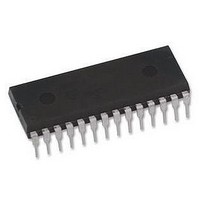
HN58C256AP85E Renesas Electronics America, HN58C256AP85E Datasheet

HN58C256AP85E
Specifications of HN58C256AP85E
Related parts for HN58C256AP85E
HN58C256AP85E Summary of contents
Page 1
HN58C256A Series HN58C257A Series 256k EEPROM (32-kword × 8-bit) Ready/Busy and RES function (HN58C257A) Description 's Renesas Technology HN58C256A and HN58C257A are electrically erasable and programmable ROMs organized as 32768-word × 8-bit. They have realized high speed low power consumption ...
Page 2
HN58C256A Series, HN58C257A Series Ordering Information Type No. Access time HN58C256AP- HN58C256AP-10 100 ns HN58C256AFP- HN58C256AFP-10 100 ns HN58C256AT- HN58C256AT-10 100 ns HN58C257AT- HN58C257AT-10 100 ns HN58C256AP-85E 85 ns HN58C256AP-10E 100 ns ...
Page 3
HN58C256A Series, HN58C257A Series Pin Arrangement HN58C256AP/AFP Series A14 A12 A13 A11 ...
Page 4
HN58C256A Series, HN58C257A Series Pin Description Pin name A0 to A14 I/ RDY/Busy* RES Note: 1. This function is supported by only the HN58C257A series. Block Diagram Note: ...
Page 5
HN58C256A Series, HN58C257A Series Operation Table CE OE Operation Read ×* 2 Standby V IH Write Deselect × × Write inhibit × Data polling V V ...
Page 6
HN58C256A Series, HN58C257A Series DC Characteristics ( +70°C, V Parameter Symbol Min Input leakage current I LI Output leakage current I LO Standby V current I CC CC1 I CC2 Operating V ...
Page 7
HN58C256A Series, HN58C257A Series AC Characteristics ( +70°C, V Test Conditions • Input pulse levels • Input rise and fall time: ≤ • Input timing reference ...
Page 8
HN58C256A Series, HN58C257A Series Write Cycle Parameter Address setup time Address hold time CE to write setup time (WE controlled) CE hold time (WE controlled write setup time (CE controlled) WE hold time (CE controlled write ...
Page 9
HN58C256A Series, HN58C257A Series Timing Waveforms Read Timing Waveform Address CE OE High WE Data Out RES * 2 Rev.6.00, Oct. 26.2006, page ACC Data out valid ...
Page 10
HN58C256A Series, HN58C257A Series Byte Write Timing Waveform (1) (WE Controlled) Address Din High-Z 2 RDY/Busy * t RES RES * Rev.6.00, Oct. 26.2006, page ...
Page 11
HN58C256A Series, HN58C257A Series Byte Write Timing Waveform (2) (CE Controlled) Address Din High-Z 2 RDY/Busy * t RES RES * Rev.6.00, Oct. 26.2006, page ...
Page 12
HN58C256A Series, HN58C257A Series Page Write Timing Waveform (1) (WE Controlled) *7 Address A0 to A14 OES Din t DB ...
Page 13
HN58C256A Series, HN58C257A Series Page Write Timing Waveform (2) (CE Controlled) *8 Address A0 to A14 OES Din t DB ...
Page 14
HN58C256A Series, HN58C257A Series Data Polling Timing Waveform Address OEH Din X I/O7 Rev.6.00, Oct. 26.2006, page Dout OES t ...
Page 15
HN58C256A Series, HN58C257A Series Toggle bit This device provide another function to determine the internal programming cycle. If the EEPROM is set to read mode during the internal programming cycle, I/O6 will charge from “1” to “0” (toggling) for each ...
Page 16
HN58C256A Series, HN58C257A Series Software Data Protection Timing Waveform (1) (in protection mode Address 5555 Data AA Software Data Protection Timing Waveform (2) (in non-protection mode Address 5555 2AAA Data AA 55 ...
Page 17
HN58C256A Series, HN58C257A Series Functional Description Automatic Page Write Page-mode write feature allows bytes of data to be written into the EEPROM in a single write cycle. Following the initial byte cycle, an additional ...
Page 18
HN58C256A Series, HN58C257A Series Write/Erase Endurance and Data Retention Time 5 The endurance is 10 cycles in case of the page programming and 10 (1% cumulative failure rate). The data retention time is more than 10 years when a device ...
Page 19
HN58C256A Series, HN58C257A Series 2. Data Protection at V On/Off CC When V is turned on or off, noise on the control pins generated by external circuits (CPU, etc) may act trigger and turn the EEPROM to ...
Page 20
HN58C256A Series, HN58C257A Series 3. Software data protection To prevent unintentional programming, this device has the software data protection (SDP) mode. The SDP is enabled by inputting the following 3 bytes code and write data. SDP is not enabled if ...
Page 21
HN58C256A Series, HN58C257A Series Package Dimensions HN58C256AP Series (PRDP0028AB-A / Previous Code: DP-28, DP-28V) JEITA Package Code RENESAS Code Previous Code P-DIP28-13.4x35.6-2.54 PRDP0028AB-A DP-28/DP-28V Rev.6.00, Oct. 26.2006, page MASS[Typ.] 4. ...
Page 22
HN58C256A Series, HN58C257A Series Package Dimensions (cont.) HN58C256AFP Series (PRSP0028DC-A / Previous Code: FP-28D, FP-28DV) JEITA Package Code RENESAS Code Previous Code P-SOP28-8.4x18.3-1.27 PRSP0028DC Index mark Rev.6.00, Oct. 26.2006, page MASS[Typ.] FP-28D ...
Page 23
HN58C256A Series, HN58C257A Series Package Dimensions (cont.) HN58C256AT Series (PTSA0028ZB-A / Previous Code: TFP-28DB, TFP-28DBV) JEITA Package Code RENESAS Code P-TSOP(1)28-8x11.8-0.55 PTSA0028ZB-A TFP-28DB/TFP-28DBV Index mark Rev.6.00, Oct. 26.2006, page Previous Code ...
Page 24
HN58C256A Series, HN58C257A Series Package Dimensions (cont.) HN58C257AT Series (PTSA0032KD-A / Previous Code: TFP-32DA, TFP-32DAV) JEITA Package Code RENESAS Code Previous Code P-TSOP(1)32-8x12.4-0.50 PTSA0032KD-A TFP-32DA/TFP-32DAV Index mark Rev.6.00, Oct. 26.2006, page ...
Page 25
Revision History Rev. Date Contents of Modification Page Description 0.0 Jun. 19. 1995 Initial issue 1.0 May. 17. 1996 Change of format 4 Absolute Maximun Ratings Addition of note 4 4 Recommended DC Operating Conditions ...
Page 26
Notes: 1. This document is provided for reference purposes only so that Renesas customers may select the appropriate Renesas products for their use. Renesas neither makes warranties or representations with respect to the accuracy or completeness of the information contained ...


