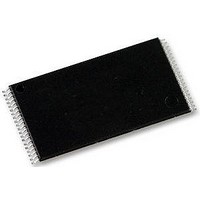
S29AL032D90TFI000 Spansion Inc., S29AL032D90TFI000 Datasheet - Page 62

S29AL032D90TFI000
Manufacturer Part Number
S29AL032D90TFI000
Description
Flash Memory IC
Manufacturer
Spansion Inc.
Specifications of S29AL032D90TFI000
Memory Size
32Mbit
Memory Configuration
4M X 8
Ic Interface Type
CFI, Parallel
Access Time
90ns
Supply Voltage Range
2.7 To 3.6 V
Memory Case Style
TSOP
No. Of Pins
40
Memory Type
Uniform Sector Flash
Interface Type
CFI
Rohs Compliant
Yes
Cell Type
NOR
Density
32Mb
Access Time (max)
90ns
Boot Type
Top
Address Bus
22/21Bit
Operating Supply Voltage (typ)
3/3.3V
Operating Temp Range
-40C to 85C
Package Type
TSOP
Sync/async
Asynchronous
Operating Temperature Classification
Industrial
Operating Supply Voltage (min)
2.7V
Operating Supply Voltage (max)
3.6V
Word Size
8/16Bit
Number Of Words
4M/2M
Supply Current
35mA
Mounting
Surface Mount
Pin Count
48
Lead Free Status / Rohs Status
Compliant
Available stocks
Company
Part Number
Manufacturer
Quantity
Price
18. Erase and Programming Performance
Notes
1. Typical program and erase times assume the following conditions: 25
2. Under worst case conditions of 90°C, V
3. The typical chip programming time is considerably less than the maximum chip programming time listed, since most bytes program faster than the maximum
4. In the pre-programming step of the Embedded Erase algorithm, all bytes are programmed to 00h before erasure.
5. System-level overhead is the time required to execute the two- or four-bus-cycle sequence for the program command. See
6. The device has a minimum erase and program cycle endurance of 100,000 cycles per sector.
7. At extended temperature range (>+85°C), typical erase time is 1.75 s and maximum erase time is 25 s.
8. At extended temperature range (>+85°C), typical erase time is 112 s.
19. TSOP and BGA Pin Capacitance
Notes
1. Sampled, not 100% tested.
2. Test conditions T
60
Sector Erase Time
Chip Erase Time
Byte Programming Time
Word Programming Time
Accelerated Byte/Word Programming Time
Chip Programming Time
(Note 3)
Parameter Symbol
program times listed.
command definitions.
C
C
C
OUT
IN2
IN
A
(Note 8)
Parameter
= 25°C, f = 1.0 MHz.
(Note 7)
Byte Mode
Word Mode
Parameter Description
Control Pin Capacitance
CC
Output Capacitance
Input Capacitance
= 2.7 V, 1,000,000 cycles.
Typ
(Note 1)
0.7
45
11
36
24
9
7
°
C, V
S29AL032D
CC
D a t a
= 3.0 V, 100,000 cycles, checkerboard data pattern.
Max
Test Setup
300
360
210
108
(Note 2)
V
10
72
V
V
OUT
IN
IN
S h e e t
= 0
= 0
= 0
Unit
Package
µs
µs
µs
TSOP
TSOP
TSOP
s
s
s
s
BGA
BGA
BGA
Excludes 00h programming
prior to erasure
Excludes system level overhead
(Note 5)
Table 11.2
S29AL032D_00_A9 January 19, 2007
Typ
4.2
8.5
5.4
7.5
3.9
6
Comments
for further information on
Max
(Note 4)
7.5
5.0
6.5
4.7
12
9
Unit
pF
pF
pF
pF
pF
pF


