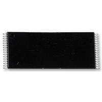
SST49LF080A-33-4C-WHE SILICON STORAGE TECHNOLOGY, SST49LF080A-33-4C-WHE Datasheet - Page 19

SST49LF080A-33-4C-WHE
Manufacturer Part Number
SST49LF080A-33-4C-WHE
Description
MEMORY, FLASH, 8M, SERIAL, 32TSOP
Manufacturer
SILICON STORAGE TECHNOLOGY
Datasheet
1.SST49LF080A-33-4C-WHE.pdf
(49 pages)
Specifications of SST49LF080A-33-4C-WHE
Memory Size
8Mbit
Clock Frequency
33MHz
Access Time
120ns
Supply Voltage Range
3V To 3.6V
Memory Case Style
TSOP
No. Of Pins
32
Operating Temperature Range
0°C To +70°C
Svhc
No SVHC
Memory Type
Flash
Memory Configuration
1024K X 8
Interface Type
Serial
Rohs Compliant
Yes
Lead Free Status / RoHS Status
Lead free / RoHS Compliant
Available stocks
Company
Part Number
Manufacturer
Quantity
Price
Company:
Part Number:
SST49LF080A-33-4C-WHE
Manufacturer:
SST
Quantity:
1 815
Part Number:
SST49LF080A-33-4C-WHE
Manufacturer:
SST
Quantity:
20 000
8 Mbit LPC Flash
SST49LF080A
Data Protection (PP Mode)
The SST49LF080A devices provide both hardware and
software features to protect nonvolatile data from inadvert-
ent writes.
Hardware Data Protection
Noise/Glitch Protection: A WE# pulse of less than 5 ns will
not initiate a Write cycle.
V
inhibited when V
Write Inhibit Mode: Forcing OE# low, WE# high will inhibit
the Write operation. This prevents inadvertent writes during
power-up or power-down.
©2006 Silicon Storage Technology, Inc.
DD
Power Up/Down Detection: The Write operation is
DD
is less than 1.5V.
19
Software Data Protection (SDP)
The SST49LF080A provides the JEDEC approved Soft-
ware Data Protection scheme for all data alteration opera-
tion, i.e., Program and Erase. Any Program operation
requires the inclusion of a series of three-byte sequence.
The three-byte load sequence is used to initiate the Pro-
gram operation, providing optimal protection from inadvert-
ent Write operations, e.g., during the system power-up or
power-down. Any Erase operation requires the inclusion of
a six-byte load sequence.
S71235-02-000
Data Sheet
5/06


