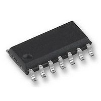
FM31274-G Ramtron, FM31274-G Datasheet - Page 16

FM31274-G
Manufacturer Part Number
FM31274-G
Description
FRAM, MPU SUPPORT, 16K, RTC, SOIC14
Manufacturer
Ramtron
Datasheet
1.FM31274-G.pdf
(26 pages)
Specifications of FM31274-G
Memory Size
16Kbit
Nvram Features
RTC
Supply Voltage Range
4V To 5.5V
Memory Case Style
SOIC
No. Of Pins
14
Operating Temperature Range
-40°C To +85°C
Interface
Serial
Package / Case
SOIC
Memory Configuration
2048 X 8
Interface Type
I2C, Serial, 2-Wire
Rohs Compliant
Yes
Lead Free Status / RoHS Status
Lead free / RoHS Compliant
Available stocks
Company
Part Number
Manufacturer
Quantity
Price
Company:
Part Number:
FM31274-GTR
Manufacturer:
CYPRESS
Quantity:
2 500
Part Number:
FM31274-GTR
Manufacturer:
RAMTRON
Quantity:
20 000
Two-wire Interface
The FM31L27x employs an industry standard two-
wire bus that is familiar to many users. This product
is unique since it incorporates two logical devices in
one chip. Each logical device can be accessed
individually. Although monolithic, it appears to the
system software to be two separate products. One is
a memory device. It has a Slave Address (Slave ID =
1010b) that operates the same as a stand-alone
memory device. The second device is a real-time
clock and processor companion which have a unique
Slave Address (Slave ID = 1101b).
Start Condition
A Start condition is indicated when the bus master
drives SDA from high to low while the SCL signal is
high. All read and write transactions begin with a
Start condition. An operation in progress can be
aborted by asserting a Start condition at any time.
Aborting an operation using the Start condition will
ready the FM31L27x for a new operation.
If the power supply drops below the specified VTP
during operation, any 2-wire transaction in progress
will be aborted and the system must issue a Start
condition prior to performing another operation.
Stop Condition
A Stop condition is indicated when the bus master
drives SDA from low to high while the SCL signal is
high. All operations must end with a Stop condition.
If an operation is pending when a stop is asserted,
the operation will be aborted. The master must have
control of SDA (not a memory read) in order to
assert a Stop condition.
Data/Address Transfer
All data transfers (including addresses) take place
while the SCL signal is high. Except under the two
conditions described above, the SDA signal should
not change while SCL is high.
Rev. 2.0
Jan. 2011
SDA
SCL
(Master)
Stop
(Master)
Start
Figure 11. Data Transfer Protocol
(Transmitter)
7
Data bits
By convention, any device that is sending data onto
the bus is the transmitter while the target device for
this data is the receiver. The device that is
controlling the bus is the master. The master is
responsible for generating the clock signal for all
operations. Any device on the bus that is being
controlled is a slave. The FM31L27x is always a
slave device.
The bus protocol is controlled by transition states in
the SDA and SCL signals. There are four conditions:
Start, Stop, Data bit, and Acknowledge. The figure
below illustrates the signal conditions that specify
the four states. Detailed timing diagrams are shown
in the Electrical Specifications section.
Acknowledge
The Acknowledge (ACK) takes place after the 8
data bit has been transferred in any transaction.
During this state the transmitter must release the
SDA bus to allow the receiver to drive it. The
receiver drives the SDA signal low to acknowledge
receipt of the byte. If the receiver does not drive
SDA low, the condition is a No-Acknowledge
(NACK) and the operation is aborted.
The receiver might NACK for two distinct reasons.
First is that a byte transfer fails. In this case, the
NACK ends the current operation so that the part can
be addressed again. This allows the last byte to be
recovered in the event of a communication error.
Second and most common, the receiver does not
send an ACK to deliberately terminate an operation.
For example, during a read operation, the FM31L27x
will continue to place data onto the bus as long as the
receiver sends ACKs (and clocks). When a read
operation is complete and no more data is needed,
the receiver must NACK the last byte. If the receiver
ACKs the last byte, this will cause the FM31L27x to
attempt to drive the bus on the next clock while the
master is sending a new command such as a Stop.
FM31L278/L276/L274/L272 - 3V I2C Companion
6
(Transmitter)
Data bit
0
Acknowledge
(Receiver)
Page 16 of 26
th


