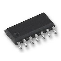
FM31274-G Ramtron, FM31274-G Datasheet - Page 3

FM31274-G
Manufacturer Part Number
FM31274-G
Description
FRAM, MPU SUPPORT, 16K, RTC, SOIC14
Manufacturer
Ramtron
Datasheet
1.FM31274-G.pdf
(26 pages)
Specifications of FM31274-G
Memory Size
16Kbit
Nvram Features
RTC
Supply Voltage Range
4V To 5.5V
Memory Case Style
SOIC
No. Of Pins
14
Operating Temperature Range
-40°C To +85°C
Interface
Serial
Package / Case
SOIC
Memory Configuration
2048 X 8
Interface Type
I2C, Serial, 2-Wire
Rohs Compliant
Yes
Lead Free Status / RoHS Status
Lead free / RoHS Compliant
Available stocks
Company
Part Number
Manufacturer
Quantity
Price
Company:
Part Number:
FM31274-GTR
Manufacturer:
CYPRESS
Quantity:
2 500
Part Number:
FM31274-GTR
Manufacturer:
RAMTRON
Quantity:
20 000
Pin Descriptions
Rev. 2.0
Jan. 2011
Pin Name
A0, A1
CNT1,
CNT2
CAL/PFO
X1, X2
/RST
SDA
SCL
PFI
VBAK
VDD
VSS
CAL/PFO
A1, A0
VBAK
VDD
SDA
SCL
RST
PFI
2.5V
Output
Supply
Supply
Supply
Type
Input
Input
Input
Input
I/O
I/O
I/O
Interface
2-Wire
LockOut
+
-
Pin Description
Device select inputs are used to address multiple memories on a serial bus. To select the
device the address value on the two pins must match the corresponding bits contained in
the device address. The device select pins are pulled down internally.
Event Counter Inputs: These battery-backed inputs increment counters when an edge is
detected on the corresponding CNT pin. The polarity is programmable. These pins
should not be left floating. Tie to ground if these pins are not used.
In calibration mode, this pin supplies a 512 Hz square-wave output for clock calibration.
In normal operation, this is the early power-fail output.
32.768 kHz crystal connection. When using an external oscillator, apply the clock to X1
and a DC mid-level to X2 (see Crystal Oscillator section for suggestions).
Active low reset output with weak pull-up. Also input for manual reset.
Serial Data & Address: This is a bi-directional line for the two-wire interface. It is open-
drain and is intended to be wire-OR’d with other devices on the two-wire bus. The input
buffer incorporates a Schmitt trigger for noise immunity and the output driver includes
slope control for falling edges. A pull-up resistor is required.
Serial Clock: The serial clock line for the two-wire interface. Data is clocked out of the
part on the falling edge, and in on the rising edge. The SCL input also incorporates a
Schmitt trigger input for noise immunity.
Early Power-fail Input: Typically connected to an unregulated power supply to detect an
early power failure. This pin should not be left floating.
Backup supply voltage: A 3V battery or a large value capacitor. If no backup supply is
used, this pin should be tied to ground and the VBC bit should be cleared. The trickle
charger is UL recognized and ensures no excessive current when using a lithium battery.
Supply Voltage
Ground
+
-
1.2V
Watchdog
LV Detect
Figure 1. Block Diagram
512Hz
Switched Power
RTC Cal.
Registers
Function
Special
Nonvolatile
S/N
FM31L278/L276/L274/L272 - 3V I2C Companion
LockOut
RTC Registers
Counters
Battery Backed
F-RAM
Event
RTC
Array
X1
X2
Page 3 of 26
CNT1
CNT2


