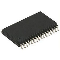
IS62WV1288BLL-55HLI INTEGRATED SILICON SOLUTION (ISSI), IS62WV1288BLL-55HLI Datasheet - Page 3

IS62WV1288BLL-55HLI
Manufacturer Part Number
IS62WV1288BLL-55HLI
Description
IC, SRAM, 1MBIT, 55NS, TSOP-32
Manufacturer
INTEGRATED SILICON SOLUTION (ISSI)
Datasheet
1.IS62WV1288BLL-55HLI.pdf
(15 pages)
Specifications of IS62WV1288BLL-55HLI
Memory Size
2Mbit
Memory Configuration
128K X 16
Access Time
55ns
Supply Voltage Range
2.5V To 3.6V
Memory Case Style
TSOP
No. Of Pins
32
Operating Temperature Range
-40°C To +85°C
Lead Free Status / RoHS Status
Lead free / RoHS Compliant
Available stocks
Company
Part Number
Manufacturer
Quantity
Price
Company:
Part Number:
IS62WV1288BLL-55HLI
Manufacturer:
ISSI
Quantity:
80
Company:
Part Number:
IS62WV1288BLL-55HLI
Manufacturer:
ISSI
Quantity:
1 000
Company:
Part Number:
IS62WV1288BLL-55HLI
Manufacturer:
PHILIPS
Quantity:
10 837
Part Number:
IS62WV1288BLL-55HLI
Manufacturer:
ISSI
Quantity:
20 000
IS62WV1288ALL, IS62WV1288BLL, IS65WV1288BLL
ABSOLUTE MAXIMUM RATINGS
Note:
1. Stress greater than those listed under ABSOLUTE MAXIMUM RATINGS may cause permanent damage to the device. This is a
OPERATING RANGE (V
DC ELECTRICAL CHARACTERISTICS
Notes:
1. Undershoot: –1.0V for pulse width less than 10 ns. Not 100% tested.
2. Overshoot: V
TRUTH TABLE
Integrated Silicon Solution, Inc. — www.issi.com —
Rev. E
11/12/08
Symbol
V
V
t
P
stress rating only and functional operation of the device at these or any other conditions above those indicated in the operational
sections of this specification is not implied. Exposure to absolute maximum rating conditions for extended periods may affect reli-
ability.
Range
Commercial
Industrial/A1
Automotive
Symbol
V
V
V
V
I
I
Mode
Not Selected
(Power-down)
Output Disabled
Read
Write
LI
Lo
stg
term
dd
t
oh
oL
Ih
IL
(1)
(2)
Parameter
Output HIGH Voltage
Output LOW Voltage
Input HIGH Voltage
Input LOW Voltage
Input Leakage
Output Leakage
dd
+ 1.0V for pulse width less than 10 ns. Not 100% tested.
Ambient Temperature
Parameter
Terminal Voltage with Respect to GND
V
Storage Temperature
Power Dissipation
dd
–40°C to +125°C
–40°C to +85°C
WE
0°C to +70°C
Related to GND
X
X
H
H
L
dd
)
CS1
H
X
L
L
L
Test Conditions
I
I
I
I
GND ≤ V
GND ≤ V
oh
oh
oL
oL
(1)
CS2
H
H
H
X
L
= 0.1 mA
= 2.1 mA
= -0.1 mA
= -1 mA
(Over Operating Range)
In
out
OE
X
X
H
X
L
≤ V
IS62WV1288ALL
≤ V
dd
1-800-379-4774
1.65V - 2.2V
1.65V - 2.2V
dd
, Outputs Disabled
I/O Operation
High-Z
High-Z
High-Z
d
d
out
1.65-2.2V
1.65-2.2V
1.65-2.2V
1.65-2.2V
In
2.5-3.6V
2.5-3.6V
2.5-3.6V
2.5-3.6V
–0.2 to V
V
–0.2 to +3.8
–65 to +150
dd
Value
1.0
dd
+0.3
IS62/65WV1288BLL
V
dd
I
sB
Min.
–0.2
–0.2
2.5V - 3.6V
2.5V - 3.6V
2.5V - 3.6V
1.4
2.2
1.4
2.2
–1
–1
—
—
Current
1
I
I
I
cc
cc
cc
, I
sB
I
sB
2
1
, I
sB
Unit
V
V
°C
W
V
V
dd
dd
2
Max.
0.2
0.4
0.4
0.6
—
—
1
1
+ 0.2
+ 0.3
Unit
µA
µA
V
V
V
V
V
V
V
V
3


