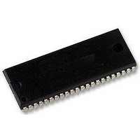
IDT71V416S12PHG INTEGRATED DEVICE TECHNOLOGY, IDT71V416S12PHG Datasheet - Page 4

IDT71V416S12PHG
Manufacturer Part Number
IDT71V416S12PHG
Description
SRAM, ASYCH, 4M, 256KX16, TSOP44
Manufacturer
INTEGRATED DEVICE TECHNOLOGY
Datasheet
1.IDT71V416S12PHG8.pdf
(9 pages)
Specifications of IDT71V416S12PHG
Memory Size
4Mbit
Access Time
12ns
Supply Voltage Range
3V To 3.6V
Memory Case Style
TSOP
No. Of Pins
44
Operating Temperature Range
0°C To +70°C
Operating Temperature Max
+70°C
Operating
RoHS Compliant
Memory Configuration
256K X 16
Rohs Compliant
Yes
Available stocks
Company
Part Number
Manufacturer
Quantity
Price
Part Number:
IDT71V416S12PHG
Manufacturer:
IDT
Quantity:
20 000
Part Number:
IDT71V416S12PHGI
Manufacturer:
IDT
Quantity:
20 000
DC Electrical Characteristics
(V
DC Electrical Characteristics
(V
AC Test Loads
NOTES:
1. All values are maximum guaranteed values.
2. All inputs switch between 0.2V (Low) and V
3. Power specifications are preliminary.
4. fMAX = 1/t
5. Standard power 10ns (S10) speed grade only.
IDT71V416S, IDT71V416L, 3.3V CMOS Static RAM
4 Meg (256K x 16-Bit)
DD
DD
Symbol
Symbol
= Min. to Max., Commercial and Industrial Temperature Ranges)
V
= Min. to Max., V
|I
V
I
|I
I
I
SB1
CC
SB
I/O
LO
OH
OL
LI
(Typical, ns)
|
|
∆t
AA,
t
RC
ACS
(all address inputs are cycling at f
Input Leakage Current
Dynamic Operating Current
Dynamic Standby Power Supply Current
Full Standby Pow er Supply Current (static)
Output Leakage Current
Output Low Voltage
Output High Voltage
CS < V
CS > V
CS > V
7
6
5
4
3
2
1
Figure 3. Output Capacitive Derating
•
8
Z
20 40 60 80 100 120 140 160 180 200
•
0
LC
HC
HC
Figure 1. AC Test Load
•
= 50Ω
LC
, Outputs Open, V
, Outputs Open, V
, Outputs Open, V
•
= 0.2V, V
CAPACITANCE (pF)
•
Parameter
•
Parameter
HC
IDT71V416S/71V416L
+1.5V
= V
DD
DD
DD
DD
= Max., f = f
DD
= Max., f = f
= Max., f = 0
50Ω
-0.2V (High).
MAX
30pF
– 0.2V)
); f = 0 means no address input lines are changing.
3624 drw 05
•
MAX
MAX
(4)
3624 drw 03
(1, 2, 3)
(4)
(4)
I
I
V
V
OL
OH
CC
DD
= 8mA, V
= -4mA, V
= Max., V
= Max., CS = V
S
L
S
L
S
L
6.42
4
AC Test Conditions
DD
Input Pulse Levels
Input Rise/Fall Times
Input Timing Reference Levels
Output Reference Levels
AC Test Load
Com'l.
DD
IN =
200
180
70
50
20
71V416S/L10
10
= Min.
= Min.
V
Test Conditions
SS
IH
, V
DATA
to V
OUT
Ind.
200
DD
—
70
—
20
—
= V
(5)
OUT
Commercial and Industrial Temperature Ranges
*Including jig and scope capacitance.
5pF*
SS
(for t
to V
Com'l.
180
170
Figure 2. AC Test Load
60
45
20
71V416S/L12
10
CLZ
DD
, t
OLZ
, t
CHZ
Ind.
180
170
60
20
, t
45
10
3.3V
OHZ
, t
OW
320Ω
350Ω
, and t
Min.
Com'l.
2.4
___
___
___
170
160
50
20
40
10
71V416S/L15
IDT71V416
WHZ
)
Figures 1,2 and 3
GND to 3.0V
3624 drw 04
Max.
0.4
Ind.
170
160
___
1.5ns
50
40
20
1.5V
1.5V
10
5
5
3624 tbl 08
3624 tbl 07
3624 tbl 09
Unit
Unit
mA
mA
mA
µ A
µ A
V
V


