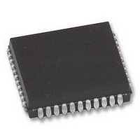
AT80C51RD2-SLSUM Atmel, AT80C51RD2-SLSUM Datasheet - Page 72

AT80C51RD2-SLSUM
Manufacturer Part Number
AT80C51RD2-SLSUM
Description
MCU, 8BIT, 8051, 5V, SPI, 20MHZ, 44PLCC
Manufacturer
Atmel
Specifications of AT80C51RD2-SLSUM
Controller Family/series
(8051) 8052
No. Of I/o's
32
Ram Memory Size
1280Byte
Cpu Speed
40MHz
No. Of Timers
3
No. Of Pwm Channels
5
Core Size
8bit
Oscillator Type
External Only
Processor Series
AT80x
Core
8051
Data Bus Width
8 bit
Program Memory Type
ROMLess
Data Ram Size
1280 B
Interface Type
UART, SPI
Maximum Clock Frequency
60 MHz
Number Of Programmable I/os
32
Number Of Timers
3
Operating Supply Voltage
2.7 V to 5.5 V
Maximum Operating Temperature
+ 85 C
Mounting Style
SMD/SMT
Package / Case
PLCC
3rd Party Development Tools
PK51, CA51, A51, ULINK2
Minimum Operating Temperature
- 40 C
Cpu Family
AT80
Device Core
8051
Device Core Size
8b
Frequency (max)
40MHz
Program Memory Size
Not Required
Total Internal Ram Size
1.25KB
# I/os (max)
32
Number Of Timers - General Purpose
3
Operating Supply Voltage (typ)
3.3/5V
Operating Supply Voltage (max)
5.5V
Operating Supply Voltage (min)
2.7V
Instruction Set Architecture
CISC
Operating Temp Range
-40C to 85C
Operating Temperature Classification
Industrial
Mounting
Surface Mount
Pin Count
44
Package Type
PLCC
Lead Free Status / RoHS Status
Lead free / RoHS Compliant
Lead Free Status / RoHS Status
Lead free / RoHS Compliant
Available stocks
Company
Part Number
Manufacturer
Quantity
Price
Company:
Part Number:
AT80C51RD2-SLSUM
Manufacturer:
Atmel
Quantity:
1 445
17.3.8
17.3.9
17.3.10
4113D–8051–01/09
Shift Register Timing Waveforms
External Clock Drive Waveforms
AC Testing Input/Output Waveforms
INSTRUCTION
ALE
CLOCK
OUTPUT DATA
WRITE to SBUF
INPUT DATA
CLEAR RI
Table 17-9.
AC inputs during testing are driven at V
measurement are made at V
T
QVXH
0
INPUT/OUTPUT
0.45V
T
XHDV
V
CC
1
-0.5V
0
AC Parameters for a Variable Clock
VALID
T
XLXL
T
XHQX
2
1
0.2V
VALID
0.7V
Symbol
CC
T
T
T
T
T
QVHX
XHQX
XHDX
XHDV
IH
XLXL
CC
-0.1
T
V
CHCL
T
CC
min for a logic “1” and V
3
XHDX
2
0.45V
-0.5V
VALID
Type
Max
Min
Min
Min
Min
4
CC
3
VALID
- 0.5 for a logic “1” and 0.45V for a logic “0”. Timing
Standard
10 T - x
10 T - x
Clock
2 T - x
T
12 T
CLCX
x
5
4
VALID
IL
0.2 V
0.2 V
X2 Clock
5 T - x
max for a logic “0”.
5 T- x
T - x
T
6 T
6
x
5
CLCL
CC
CC
VALID
+ 0.9
- 0.1
T
CLCH
X Parameter for -
T
7
6
CHCX
VALID
M Range
AT80C51RD2
133
50
20
0
SET TI
SET RI
8
7
VALID
Units
ns
ns
ns
ns
ns
69


