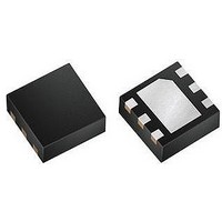
LT3493EDCB#PBF Linear Technology, LT3493EDCB#PBF Datasheet - Page 7

LT3493EDCB#PBF
Manufacturer Part Number
LT3493EDCB#PBF
Description
IC, STEP-DOWN PWM DC/DC CONVERTER, DFN-6
Manufacturer
Linear Technology
Datasheet
1.LT3493EDCBTRMPBF.pdf
(20 pages)
Specifications of LT3493EDCB#PBF
Primary Input Voltage
36V
No. Of Outputs
1
Output Current
1.2A
No. Of Pins
6
Operating Temperature Range
-40°C To +85°C
Supply Voltage Range
3.6V To 36V
Switching Frequency Max
815kHz
Msl
MSL 1 - Unlimited
Rohs Compliant
Yes
Lead Free Status / RoHS Status
Lead free / RoHS Compliant
Available stocks
Company
Part Number
Manufacturer
Quantity
Price
OPERATION
The LT3493 is a constant frequency, current mode step-
down regulator. A 750kHz oscillator enables an RS fl ip-fl op,
turning on the internal 1.75A power switch Q1. An amplifi er
and comparator monitor the current fl owing between the
V
reaches a level determined by the voltage at V
amplifi er measures the output voltage through an external
resistor divider tied to the FB pin and servos the V
If the error amplifi er’s output increases, more current is
delivered to the output; if it decreases, less current is
delivered. An active clamp (not shown) on the V
provides current limit. The V
the voltage on the SHDN pin; soft-start is implemented
by generating a voltage ramp at the SHDN pin using an
external resistor and capacitor.
IN
and SW pins, turning the switch off when this current
(Refer to Block Diagram)
C
node is also clamped to
C
. An error
C
C
node.
node
An internal regulator provides power to the control circuitry.
This regulator includes an undervoltage lockout to prevent
switching when V
used to place the LT3493 in shutdown, disconnecting the
output and reducing the input current to less than 2μA.
The switch driver operates from either the input or from
the BOOST pin. An external capacitor and diode are used
to generate a voltage at the BOOST pin that is higher than
the input supply. This allows the driver to fully saturate the
internal bipolar NPN power switch for effi cient operation.
The oscillator reduces the LT3493’s operating frequency
when the voltage at the FB pin is low. This frequency
foldback helps to control the output current during start-
up and overload.
IN
is less than ~3.4V. The SHDN pin is
LT3493
3493fb
7


