BD4154FV-E2 Rohm Semiconductor, BD4154FV-E2 Datasheet - Page 25
BD4154FV-E2
Manufacturer Part Number
BD4154FV-E2
Description
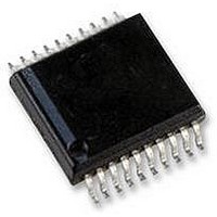
POWER SWITCH EXPRESS CARD, SSOP-B20
Manufacturer
Rohm Semiconductor
Series
-r
Specifications of BD4154FV-E2
Primary Input Voltage
3.6V
No. Of Outputs
1
Output Voltage
5V
Output Current
1.3A
Voltage Regulator Case Style
SSOP
No. Of Pins
20
Operating Temperature Range
-40°C To +100°C
Svhc
No SVHC
Applications
PCMCIA, ExpressCard™
Current - Supply
250µA
Voltage - Supply
3 V ~ 3.6 V
Operating Temperature
-40°C ~ 100°C
Mounting Type
Surface Mount
Package / Case
20-TSSOP (0.173", 4.40mm Width)
Lead Free Status / RoHS Status
Lead free / RoHS Compliant


14. Not of a radiation-resistant design.
11. Electrical characteristics
12. Capacitors to be applied to the input terminals
13. Capacitors to be applied to the output terminals
20. Heat sink
10. GND wiring pattern
15.
16. In the event that load containing a large inductance component is connected to the output terminal, and generation of
17. Operating ranges
18. We are certain that examples of applied circuit diagrams are recommendable, but you are requested to thoroughly confirm
19. Wiring to the input terminals (V3 IN, V3AUX IN, and V15 IN) and output terminals (V3, V3AUX and V15) of built-in FET
If there are a small signal GND and a high current GND, it is recommended to separate the patterns for the high current
GND and the small signal GND and provide a proper grounding to the reference point of the set not to affect the voltage at
the small signal GND with the change in voltage due to resistance component of pattern wiring and high current. Also for
GND wiring pattern of component externally connected, pay special attention not to cause undesirable change to it.
The electrical characteristics in the Specifications may vary depending on ambient temperature, power supply voltage,
circuit(s) externally applied, and/or other conditions. It is therefore requested to carefully check them including transient
characteristics.
The capacitors to be applied to the input terminals (VCC, V3_IN, V3AUX_IN and V15_IN) are used to lower the output
impedance of the power supply to be connected. An increase in the output impedance of the power supply may result in
destabilization of input voltages (VCC, V3_IN, V3AUX_IN and V15_IN). It is recommended to use a low ESR capacitor
with less temperature coefficient (change in capacitance vs. change in temperature), 0.1 µF more or less for VCC and
V3AUX_IN while 1 µF more or less for V3_IN and V15_IN, but it must be thoroughly checked at the temperature and with
the load of the range expected to use because it significantly depends on the characteristics of the input power supply to be
used and the conductor pattern of the pc board.
To the output terminals (V3, V3_AUX, and V15), the output capacitors should be connected between the respective output
terminal and GND. It is recommended to use a low ESR capacitor with less temperature coefficient, 1 µF more or less for
V3 and V15 terminals while 1µF more or less for V3_AUX, but it must be thoroughly checked at the temperature and with
the load of the range expected to use because it significantly depends on the temperature and the load conditions.
With respect to the allowable loss, the thermal derating characteristics are shown in the Exhibit, which we hope would be
used as a good-rule-of-thumb. Should the IC be used in such a manner to exceed the allowable loss, reduction of
current capacity due to chip temperature rise, and other degraded properties inherent to the IC would result. You are
strongly urged to use the IC within the allowable loss.
back-EMF at the start-up and when output is turned OFF is assumed, it is requested to insert a protection diode.
.
Allowable loss Pd
If it is within the operating ranges, certain circuit functions and operations are warranted in the working ambient
temperature range.
characteristics but there are no sudden variations in characteristic values within these ranges.
the characteristics before using the IC.In addition, when the IC is used with the external circuit changed, decide the IC with
sufficient margin provided while consideration is being given not only to static characteristics but also variations of external
parts and our IC including transient
should be carried out with special care. Unnecessarily long and/or thin conductors used in wiring may result in
degradation of characteristics including decrease in output voltage.
Heat sink is connected to SUB, which should be short-circuited to GND. Solder the heat sink to a pc board properly,
which offers lower thermal resistance.
With respect to characteristic values, it is unable to warrant standard values of electric
OUTPUT PIN
25/28
Related parts for BD4154FV-E2
Image
Part Number
Description
Manufacturer
Datasheet
Request
R

Part Number:
Description:
Manufacturer:
Rohm Semiconductor
Datasheet:
Part Number:
Description:
Manufacturer:
Rohm Semiconductor
Datasheet:
Part Number:
Description:
Manufacturer:
Rohm Semiconductor
Datasheet:
Part Number:
Description:
Manufacturer:
Rohm Semiconductor
Datasheet:
Part Number:
Description:
Manufacturer:
Rohm Semiconductor
Datasheet:
Part Number:
Description:
Manufacturer:
Rohm Semiconductor
Datasheet:
Part Number:
Description:
Manufacturer:
Rohm Semiconductor
Datasheet:
Part Number:
Description:
Manufacturer:
Rohm Semiconductor
Datasheet:
Part Number:
Description:
Manufacturer:
Rohm Semiconductor
Datasheet:
Part Number:
Description:
Manufacturer:
Rohm Semiconductor
Datasheet:
Part Number:
Description:
Manufacturer:
Rohm Semiconductor
Datasheet:
Part Number:
Description:
Manufacturer:
Rohm Semiconductor
Datasheet:

Part Number:
Description:
DIODE SWITCH 80V 25MA SMD5 TR
Manufacturer:
Rohm Semiconductor
Datasheet: