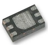
LTC4357IDCB#PBF Linear Technology, LTC4357IDCB#PBF Datasheet - Page 3

LTC4357IDCB#PBF
Manufacturer Part Number
LTC4357IDCB#PBF
Description
CONTROLLER, DIODE, SMD, DFN-6, 4357
Manufacturer
Linear Technology
Datasheet
1.LTC4357IDCBPBF.pdf
(12 pages)
Specifications of LTC4357IDCB#PBF
Primary Input Voltage
80V
No. Of Outputs
1
Output Voltage
80V
Output Current
80µA
Voltage Regulator Case Style
DFN
No. Of Pins
6
Operating Temperature Range
-40°C To +85°C
Svhc
No SVHC
Lead Free Status / RoHS Status
Lead free / RoHS Compliant
Available stocks
Company
Part Number
Manufacturer
Quantity
Price
ELECTRICAL CHARACTERISTICS
temperature range, otherwise specifi cations are at T
Note 1: Stresses beyond those listed under Absolute Maximum Ratings
may cause permanent damage to the device. Exposure to any Absolute
Maximum Rating condition for extended periods may affect device
reliability and lifetime.
SYMBOL
I
I
t
ΔV
GATE(UP)
GATE(DOWN)
OFF
SD
PARAMETER
External N-Channel Gate Pull Up Current V
External N-Channel Gate Pull Down
Current in Fault Condition
Gate Turn-Off Time
Source-Drain Regulation Voltage
(V
IN
– V
OUT
)
A
= 25°C. V
CONDITIONS
V
V
V
V
GATE
GATE
IN
GATE
GATE
The
– V
= V
= V
– V
– V
OUT
l
OUT
IN
IN
IN
IN
denotes the specifi cations which apply over the full operating
= 55mV
, V
+ 5V
< 1V
= 2.5V
= V
IN
Note 2: All currents into pins are positive, all voltages are referenced to
GND unless otherwise specifi ed.
Note 3: An internal clamp limits the GATE pin to a minimum of 10V above
IN or 100V above GND. Driving this pin to voltages beyond this clamp may
damage the device.
– V
DD
–
, V
OUT
|
–
–1V,
DD
= 0.1V
= 9V to 80V unless otherwise noted.
l
l
l
l
MIN
–14
10
1
TYP
–20
300
25
2
LTC4357
MAX
–26
500
55
UNITS
4357fb
3
mV
μA
ns
A


