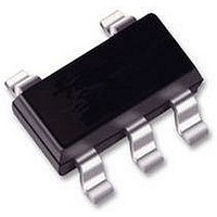
XC6220B501MR-G Torex Semiconductor Ltd, XC6220B501MR-G Datasheet - Page 10

XC6220B501MR-G
Manufacturer Part Number
XC6220B501MR-G
Description
IC, LDO, 1A, 5.0V, SOT-25
Manufacturer
Torex Semiconductor Ltd
Datasheet
1.XC6220B121ER-G.pdf
(30 pages)
Specifications of XC6220B501MR-G
Primary Input Voltage
6V
Output Voltage
5V
Dropout Voltage Vdo
655mV
No. Of Pins
5
Output Current
1A
Voltage Regulator Case Style
SOT-25
Operating Temperature Range
-40°C To +85°C
Svhc
No SVHC
Output Voltage Fixed
5V
Rohs Compliant
Yes
Lead Free Status / RoHS Status
Lead free / RoHS Compliant
10/30
The XC6220B/D series can quickly discharge the electric charge at the output capacitor (C
pin, which enables the whole IC circuit put into an OFF state, is inputted to the CE pin via the N-channel transistor located
between the V
(V
(
output capacitor value (C
by the following formulas.
<CL High Speed Auto-Discharge Function>
For the XC6220A/C series, output voltage may rises when in the high stand-by mode. Please note that in that case, the
typical characteristics may worse. When the XC6220A/C series is used, please be noted the characteristics shown below.
<Thermal Shutdown>
shutdown circuit operates and the driver transistor will be turned OFF. The IC resumes its operation when the thermal
shutdown function is released and the IC’s operation is automatically restored because the junction temperature drops to the
level of the thermal shutdown release voltage.
<Inrush Current Protection>
The XC6220 series includes an inrush current protection circuit.
The inrush current protection circuit suppresses inrush current charged to C
approximately 1 ms.
* Please note that the device can not provide the output current beyond 700 mA for a period of approximately 1 ms after the
CE pin goes high.
When the junction temperature of the built-in driver transistor reaches the temperature limit level (150℃ TYP.), the thermal
R
■OPERATIONAL EXPLANATION (Continued)
■NOTES ON USE
1
DCHG
XC6220
IN
2. Where wiring impedance is high, operations may become unstable due to noise and/or phase lag depending on output current.
3. Please wire the input capacitor (C
.
where
=6.0V, V
τ: C
Please use this IC within the stated absolute maximum ratings. The IC is liable to malfunction should the ratings be
V : Output voltage after discharge
V
t: Discharge time
exceeded.
Please strengthen V
) and the output capacitor (C
OUT(E)
1.8
1.6
1.4
1.2
1.0
0.8
0.6
0.4
0.2
0.0
L
20
auto-discharge resistance
: Output voltage
OUT
OUT
=5.0V at TYP.). The discharge time of the output capacitor (C
pin and the V
XC6220A 501x x
40
Series
L
IN
) as τ(τ=C x
and V
Ta (℃)
60
SS
SS
L
). By setting a time constant of the C
wiring in particular.
pin (cf. BLOCK DIAGRAM). The C
R
IN
DCHG
) and the output capacitor (C
80
R
×Output capacitor (C
DCHG
V = V
), the output voltage after discharge via the N channel transistor is calculated
OUT
100
x e
–t/ τ
, or t=τln( V
L
) value C)
0.7
0.6
0.5
0.4
0.3
0.2
0.1
0.0
L
Output V ol ta g e v s . Input V ol ta g e
1.0
) as close to the IC as possible.
L
auto-discharge resistance value is fixed to 460Ω
L
OUT(E)
auto-discharge resistance value [
L
2.0
when the IC starts up to 700 mA (MAX.) for
L
) is set by the C
/ V )
3.0
VIN (V)
L
), when a low signal to the CE
4.0
L
auto-discharge resistance
5.0
6.0
R
DCHG
] and an


