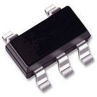
XC6220B501MR-G Torex Semiconductor Ltd, XC6220B501MR-G Datasheet - Page 9

XC6220B501MR-G
Manufacturer Part Number
XC6220B501MR-G
Description
IC, LDO, 1A, 5.0V, SOT-25
Manufacturer
Torex Semiconductor Ltd
Datasheet
1.XC6220B121ER-G.pdf
(30 pages)
Specifications of XC6220B501MR-G
Primary Input Voltage
6V
Output Voltage
5V
Dropout Voltage Vdo
655mV
No. Of Pins
5
Output Current
1A
Voltage Regulator Case Style
SOT-25
Operating Temperature Range
-40°C To +85°C
Svhc
No SVHC
Output Voltage Fixed
5V
Rohs Compliant
Yes
Lead Free Status / RoHS Status
Lead free / RoHS Compliant
CE
The XC6220 series includes a fold-back circuit, which aids the operation of the current limiter and circuit protection. When
the load current reaches the current limit level, the fold-back circuit operates and output voltage drops. As a result of this drop
in output voltage, output current also decreases. When the output pin is shorted, a current of about 180mA flows.
The IC's internal circuitry can be shutdown via the signal from the CE pin with the XC6220 series. With the XC6220B/D
series, output at the V
resistor is connected in parallel to R1 and R2 while the power supply is applied to the V
V
used with the correct output voltage for the CE pin, the logic is fixed and the IC will operate normally. However, with the
XC6220C/D series, supply current may increase as a result of through current in the IC's internal circuitry when medium
voltage is input.
<Low ESR capacitor>
the IC is used with low ESR capacitors. In order to ensure stable phase compensation it is recommended that a C
is connected as close as possible to the V
(C
Values required for the phase compensation are shown in the chart below. If a loss of the capacitance happens, the stable
phase compensation may not be obtained. Please ensure to use a capacitor which does not depend on bias or temperature
too much.
<Current Limiter, Short-Circuit Protection>
<CE Pin>
The XC6220 series has a built-in phase compensation circuit which means that a stable output voltage is achieved even if
The XC6220 series always operates in a green operation (GO) mode.
The GO mode enables the IC to switch automatically between the high
<GreenOperation>
speed (HS) mode or the power save (PS) mode according to the level of
output current. The switching point of the HS mode and the PS mode is
fixed inside the IC. When the output current becomes I
or below, the mode changes automatically to the PS mode after a delay
time of hundreds of microseconds. Supply current in light load is greatly
reduced. Also when the output current becomes I
more, the mode changes automatically to the HS mode and the IC
returns to high speed operation.
OUT
IN
■OPERATIONAL EXPLANATION
) between the V
pin reaches the V
Recommended output capacitor (C
× No option
OUTPUT VOLTAGE (V)
RCE
CE
ON/OFF
Control
circuit
each
0.80V~0.95V
1.00V~1.45V
1.50V~1.75V
1.80V~2.95V
3.00V~3.50V
3.55V~5.00V
CE/
Reference
Voltage
IN
pin and the V
OUT
SS
-
+
Operation
Error
Amp
Green
level is shortened. The output voltage becomes unstable, when the CE pin is open. If this IC is
pin will be pulled down to the V
Protection
Current
Limit
Thermal
SS
INPUT CAPACITOR VALUE
4.7μF
47μF
47μF
47μF
47μF
47μF
pin.
×
OUT
L
) Values corresponding to input capacitor (C
R1
R2
CE/
pin and V
6.8μF
4.7μF
10μF
47μF
22μF
10μF
×
GO
GOR
SS
10mA (MAX.) or
SS
6.8μF
4.7μF
6.8μF
V
=1.0mA (MIN.)
pin. For a stable power supply, please connect an input capacitor
22μF
22μF
22μF
10μF
V
V
OUT
SS
IN
level. However, with XC6220A/B series, the C
The voltage divided by resistors R1 & R2 is compared
with the internal reference voltage by the error amplifier.
The P-channel MOSFET which is connected to the V
pin is then driven by the subsequent output signal. The
output voltage at the V
by a system of negative feedback. The current limit
circuit and short protect circuit operate in relation to the
level of output current. The GO function monitors the
output current and switches the IC between two
operating modes according to the level of output
current. Further, the IC's internal circuitry can be
shutdown via the CE pin's signal.
50
40
30
20
10
0
0
IN
IN
OUT
)
pin. Therefore, the time until the
pin is controlled & stabilized
5
Output Current: I
XC6220x 301
CE=V
IN
, Topr=25℃, C
10
OUT
IN
=10μF, C
(mA)
L
15
auto-discharge
L
=4.7μF (ceramic)
L
capacitor
XC6220
OUT
20
Series
9/30


