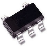
74LVC1G66GW NXP Semiconductors, 74LVC1G66GW Datasheet - Page 10

74LVC1G66GW
Manufacturer Part Number
74LVC1G66GW
Description
IC, LOGIC, 74LVC1G, SWITCH, UMT5
Manufacturer
NXP Semiconductors
Datasheet
1.74LVC1G66GW.pdf
(25 pages)
Specifications of 74LVC1G66GW
Analogue Switch Type
Bilateral Switch
No. Of Channels
1
Bandwidth
440MHz
Supply Voltage Range
1.65V To 5.5V
Operating Temperature Range
-40°C To +125°C
Analogue Switch Case Style
TSSOP
No. Of
RoHS Compliant
On State Resistance Max
23ohm
Rohs Compliant
Yes
Available stocks
Company
Part Number
Manufacturer
Quantity
Price
Company:
Part Number:
74LVC1G66GW
Manufacturer:
NXP
Quantity:
33 000
Part Number:
74LVC1G66GW
Manufacturer:
NXP/恩智浦
Quantity:
20 000
NXP Semiconductors
Table 9.
At recommended operating conditions; voltages are referenced to GND (ground = 0 V); for test circuit see
[1]
[2]
[3]
[4]
[5]
[6]
74LVC1G66
Product data sheet
Symbol Parameter
t
C
dis
Fig 16. Input (Y or Z) to output (Z or Y) propagation delays
PD
Typical values are measured at T
t
propagation delay is the calculated RC time constant of the typical ON resistance of the switch and the specified capacitance when
driven by an ideal voltage source (zero output impedance).
t
t
C
P
f
f
C
C
V
N = number of inputs switching;
Σ{(C
pd
en
dis
i
o
D
CC
PD
= input frequency in MHz;
L
S(ON)
= output frequency in MHz;
is the same as t
is the same as t
= output load capacitance in pF;
= C
is the same as t
L
is used to determine the dynamic power dissipation (P
= supply voltage in V;
+ C
disable time
power dissipation
capacitance
Measurement points are given in
Logic levels: V
PD
= maximum ON-state switch capacitance in pF;
Dynamic characteristics
S(ON)
× V
CC
11.1 Waveforms and test circuit
) × V
2
× f
PLH
PZH
PLZ
CC
i
× N + Σ{(C
OL
2
and t
and t
and t
× f
and V
o
} = sum of the outputs.
PHL
PZL
PHZ
Conditions
E to Y or Z; see
C
V
OH
I
L
L
V
V
V
V
V
V
V
V
= GND to V
+ C
= 50 pF; f
amb
are typical output voltage levels that occur with the output load.
CC
CC
CC
CC
CC
CC
CC
CC
Z or Y output
S(ON)
Y or Z input
= 1.65 V to 1.95 V
= 2.3 V to 2.7 V
= 2.7 V
= 3.0 V to 3.6 V
= 4.5 V to 5.5 V
= 2.5 V
= 3.3 V
= 5.0 V
= 25 °C and nominal V
…continued
Table
)× V
All information provided in this document is subject to legal disclaimers.
i
= 10 MHz;
CC
CC
10.
Figure 17
GND
2
V
V
× f
OH
OL
V
I
o
} where:
Rev. 7 — 30 July 2010
D
CC
in μW).
V
.
M
V
[5]
[6]
M
t
PLH
Min
1.0
1.0
1.0
1.0
1.0
-
-
-
−40 °C to +85 °C
Typ
12.0
17.3
4.2
2.4
3.6
3.4
2.5
9.8
[1]
mna667
t
PHL
Max
6.9
7.5
6.5
5.0
10
-
-
-
−40 °C to +125 °C Unit
74LVC1G66
Min
1.0
1.0
1.0
1.0
1.0
-
-
-
© NXP B.V. 2010. All rights reserved.
Figure
Bilateral switch
Max
9.0
9.5
8.5
6.5
13
-
-
-
18.
ns
ns
ns
ns
ns
pF
pF
pF
10 of 25


